Insulated gate bipolar transistor and manufacturing method thereof

A technology of bipolar transistors and manufacturing methods, which is applied in semiconductor/solid-state device manufacturing, semiconductor devices, electrical components, etc., can solve the problems of increasing conduction voltage drop and increasing turn-off time, so as to reduce turn-off time and turn-off time. The effect of breaking loss and improving recombination efficiency

Pending Publication Date: 2021-02-05
GUANGDONG MIDEA WHITE GOODS TECH INNOVATION CENT CO LTD +1
View PDF0 Cites 0 Cited by
  • Summary
  • Abstract
  • Description
  • Claims
  • Application Information

AI Technical Summary

Problems solved by technology

At present, the existing technology will increase the turn-off time while reducing the tu

Method used


Image

  • Insulated gate bipolar transistor and manufacturing method thereof
  • Insulated gate bipolar transistor and manufacturing method thereof
  • Insulated gate bipolar transistor and manufacturing method thereof

Examples


example 1

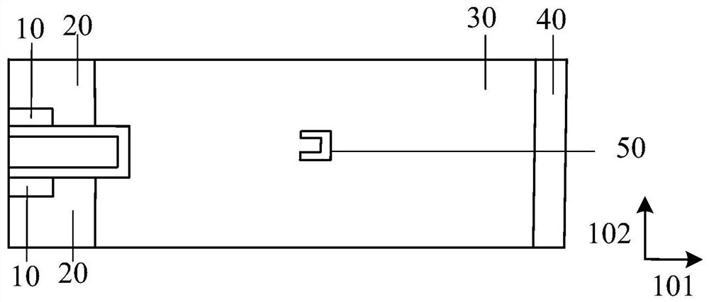
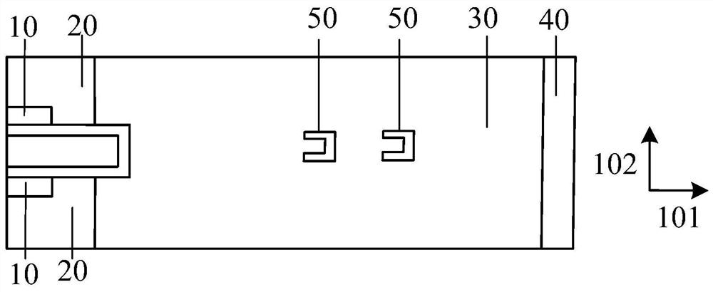
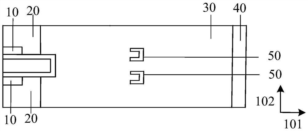
[0112] Insulated gate bipolar transistors (IGBTs) can generally be classified into lateral IGBTs and vertical IGBTs. IGBTs fabricated based on a silicon-on-insulator (SOI) process are typically lateral. Wherein, the horizontal IGBT means that the plane where the transistor structure is located is parallel to the plane where the substrate is located, and the plane where the vertical IGBT transistor structure is located is perpendicular to the plane where the substrate is located.

[0113] Figure 5 A structural diagram of an SOI lateral insulated gate bipolar transistor is shown, which includes an emitter region 10, a body region 20, a drift region 30, a collector region 40, a polysilicon gate 60, a gate oxide layer 70, and a buried oxide layer 80 and substrate 90.

[0114] When the insulated gate bipolar transistor is turned on, electrons are injected from the emitter region 10 to the drift region 30, holes are injected from the collector region 40 to the drift region 30, an...


PUM


Abstract

The embodiment of the invention discloses an insulated gate bipolar transistor and a manufacturing method thereof. The insulated gate bipolar transistor comprises an emitter region, a body region, a drift region and a collector region which are located in the same predetermined plane, wherein the body region is positioned between the emitter region and the drift region and is in contact with the emitter region and the drift region; the drift region is located between the body region and the collector region and is in contact with the collector region; at least one suppression unit is located in the drift region, comprises a concave surface with an opening facing the emitter region, and is used for suppressing at least part of carriers injected into the drift region to move towards the collector region; wherein the carriers are injected into the drift region from the emitter region, and the suppressed carriers are gathered on the surface of the suppression unit.

Description

technical field [0001] Embodiments of the present invention relate to the technical field of semiconductors, and in particular to an insulated gate bipolar transistor and a manufacturing method thereof. Background technique [0002] Insulated Gate Bipolar Transistor (IGBT for short) is a composite fully-controlled voltage-driven power semiconductor device composed of a bipolar transistor (BJT) and an insulated gate field effect transistor (MOSFET), and has a MOSFET The high input impedance of the device and the low turn-on voltage drop of the power transistor (ie giant transistor, referred to as GTR) are widely used in various fields. [0003] Turn-on voltage drop and turn-off time are important factors reflecting IGBT performance. Currently, in the prior art, the turn-off time is increased while the turn-on voltage drop is reduced, or the turn-on voltage drop is increased while the turn-off time is reduced. Contents of the invention [0004] In view of this, an embodime...

Claims


Application Information

Patent Timeline
IPC IPC(8): H01L29/739H01L29/06H01L21/331
CPCH01L29/7394H01L29/0649H01L29/66325
Inventor 兰昊冯宇翔
Owner GUANGDONG MIDEA WHITE GOODS TECH INNOVATION CENT CO LTD
Why Eureka
Try Eureka