
Electroluminescent device, preparation method thereof and display device

A technology of electroluminescent devices and light-emitting layers, which is applied in the direction of electric solid-state devices, semiconductor/solid-state device manufacturing, electrical components, etc., and can solve problems such as limiting the performance of electroluminescent devices, large work function, and restricting the effective injection and transmission of electrons

Active Publication Date: 2021-02-09
GUANGDONG JUHUA PRINTING DISPLAY TECH CO LTD
View PDF8 Cites 1 Cited by
  • Summary
  • Abstract
  • Description
  • Claims
  • Application Information

AI Technical Summary

Problems solved by technology

However, these functional materials still have significant deficiencies. Their work functions are generally large, and there is an energy barrier of at least 1eV between the LUMO energy level or the bottom energy level of the conduction band of most luminescent materials, which restricts the effective injection of electrons. and transport, which limits the performance of electroluminescent devices

Method used


Image

  • Electroluminescent device, preparation method thereof and display device
  • Electroluminescent device, preparation method thereof and display device
  • Electroluminescent device, preparation method thereof and display device

Examples


preparation example Construction

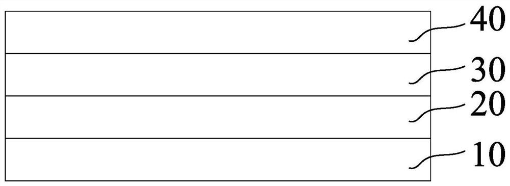
[0062] The embodiment of the present invention also provides a method for preparing an electroluminescent device, the electroluminescent device has an inverted structure, and the preparation method includes:

[0063] forming a cathode layer 10 on the substrate;

[0064] Forming the electronic functional layer 20 on the cathode layer 10, wherein the steps of forming the electronic functional layer 20 on the cathode layer 10 are:

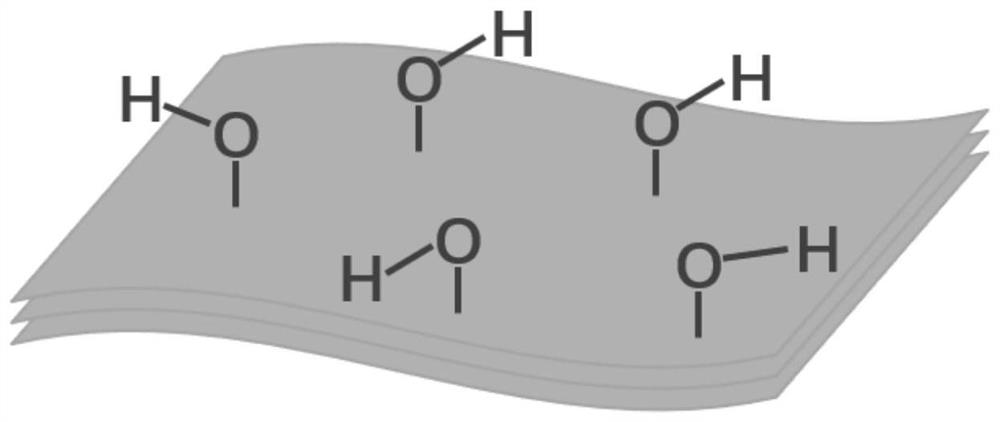
[0065] Provided is a mixed system comprising a functional material for transporting and / or injecting electrons, a hydroxyl-modified two-dimensional layered nanomaterial, and a solvent, the work function of the hydroxyl-modified two-dimensional layered nanomaterial being smaller than that of the functional material function;

[0066] depositing said hybrid system on said cathode layer 10; and

[0067] The solvent in the mixed system is removed.

[0068] In one of the embodiments, the preparation method of the electroluminescent device includes:

[...

Embodiment 1

[0092] (1) The transparent conductive film ITO is used as the cathode layer 10 with a thickness of 50 nm.

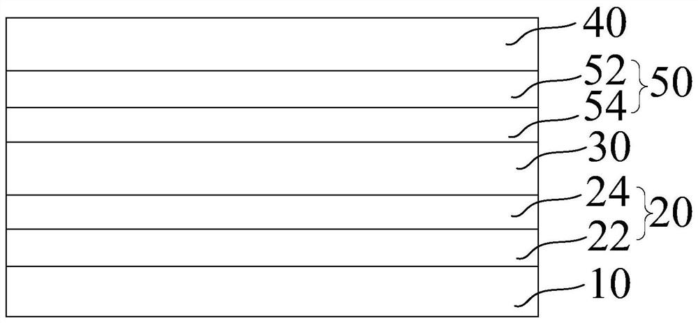
[0093] (2) The electronic functional material SnO 2 and hydroxyl-modified two-dimensional layered nanomaterials Ti 4 N 3 (OH) 2 According to the mass ratio of 0.7:0.3 dispersed in water and ethanol mixed liquid to obtain electron transport layer 24 mixed system. The mixed system of the electron transport layer 24 was coated on the cathode layer 10 with a solution, and the solvent was removed to obtain the electron transport layer 24 with a thickness of 50 nm.

[0094] (3) Deposit ZnCdS / ZnS quantum dot material as the quantum dot light-emitting layer 30 on the electron transport layer 24 by solution method, with a thickness of 25 nm.

[0095] (4) Depositing CPB as the hole transport layer 54 on the quantum dot light-emitting layer 30 by evaporation method, with a thickness of 40 nm.

[0096] (5) Deposit HAT-CN as the hole injection layer 52 on the hole transport laye...

Embodiment 2

[0099] (1) The transparent conductive film ITO is used as the cathode layer 10 with a thickness of 50 nm.

[0100] (2) The two-dimensional layered nanomaterial Ti modified by the electronic functional material ZnO and hydroxyl groups 4 N 3 (OH) 2 According to the mass ratio of 0.8:0.2 dispersed in water and ethanol mixed liquid to obtain electron transport layer 24 mixed system. The mixed system of the electron transport layer 24 was coated on the cathode layer 10 with a solution, and the solvent was removed to obtain the electron transport layer 24 with a thickness of 60 nm.

[0101] (3) Deposit ZnCdS / ZnS quantum dot material on the electron transport layer 24 as the quantum dot light-emitting layer 30 with a thickness of 30 nm by using a solution method.

[0102] (4) Deposit TCTA as the hole transport layer 54 on the quantum dot light-emitting layer 30 by evaporation method, with a thickness of 30 nm.

[0103] (5) Deposit MoO on the hole transport layer 54 by vapor depos...


PUM

PropertyMeasurementUnit
electron work functionaaaaaaaaaa
particle diameteraaaaaaaaaa
sizeaaaaaaaaaa

Abstract

The invention discloses an electroluminescent device, which comprises a cathode layer, an electronic function layer, a luminescent layer and an anode layer, and is characterized in that the cathode layer and the anode layer are oppositely arranged, the electronic function layer is arranged between the cathode layer and the anode layer, and the luminescent layer is arranged between the electronic function layer and the anode layer. The electronic function layer comprises a functional material for transmitting and / or injecting electrons and a hydroxyl-modified two-dimensional layered nano material doped in the functional material, and the work function of the hydroxyl-modified two-dimensional layered nano material is smaller than that of the functional material. The invention also disclosesa preparation method of the electroluminescent device. The invention further discloses a display device.

Description

technical field [0001] The invention relates to the technical field of light emitting devices, in particular to an electroluminescent device, a preparation method thereof and a display device. Background technique [0002] New electroluminescent devices represented by organic light-emitting diodes (OLEDs) and quantum dot light-emitting diodes (QLEDs) not only have technical characteristics that are not available in many liquid crystals (LCDs), such as light weight, flexibility, foldability, and bendability, but also It has more excellent optical characteristics such as wide color gamut, large viewing angle, and high contrast, so as to bring users a better visual experience, which also promotes the continuous development of new display technologies. [0003] Some new functional materials are being used in electroluminescent devices. For example, metal oxides are increasingly favored by people because of their good water and oxygen resistance, excellent electrical conductivity...

Claims


Application Information

Patent Timeline
Patent Type & Authority Applications(China)
IPC IPC(8): H01L51/50H01L51/54H01L51/56B82Y30/00B82Y40/00
CPCB82Y30/00B82Y40/00H10K50/115H10K50/165H10K50/171H10K2102/00H10K71/00
Inventor 苏亮
Owner GUANGDONG JUHUA PRINTING DISPLAY TECH CO LTD
Learn More