Tuned Laser Chip

A technology for tuning lasers and chips, applied in lasers, laser parts, semiconductor lasers, etc., can solve the problem of limited size of optical emission modules, achieve fine tuning and wide-range tuning avoidance, optimize L-band wide-range tuning, and optimize edge Effect of Mode Suppression Ratio

Active Publication Date: 2022-04-22
INST OF SEMICONDUCTORS - CHINESE ACAD OF SCI
View PDF5 Cites 0 Cited by
  • Summary
  • Abstract
  • Description
  • Claims
  • Application Information

AI Technical Summary

Problems solved by technology

[0003] Starting from practical applications, the wavelength division multiplexing (WDM) transmission system needs to consider the limitations of tunable light sources while considering the increase in bandwidth and capacity. How to realize a wide range of wavelength scanning light sources that meet the L-band is In recent years, a major problem that has plagued researchers, and the size of the optical transmission module in the communication system is limited, and it is a huge challenge to achieve wide-range tuning and fast switching of a single module

Method used


Image

  • Tuned Laser Chip
  • Tuned Laser Chip

Examples


Embodiment Construction

[0025] Hereinafter, embodiments of the present disclosure will be described with reference to the drawings. It should be understood, however, that these descriptions are exemplary only, and are not intended to limit the scope of the present disclosure. In the following detailed description, for purposes of explanation, numerous specific details are set forth in order to provide a thorough understanding of the embodiments of the present disclosure. It may be evident, however, that one or more embodiments may be practiced without these specific details. Also, in the following description, descriptions of well-known structures and techniques are omitted to avoid unnecessarily obscuring the concepts of the present disclosure.

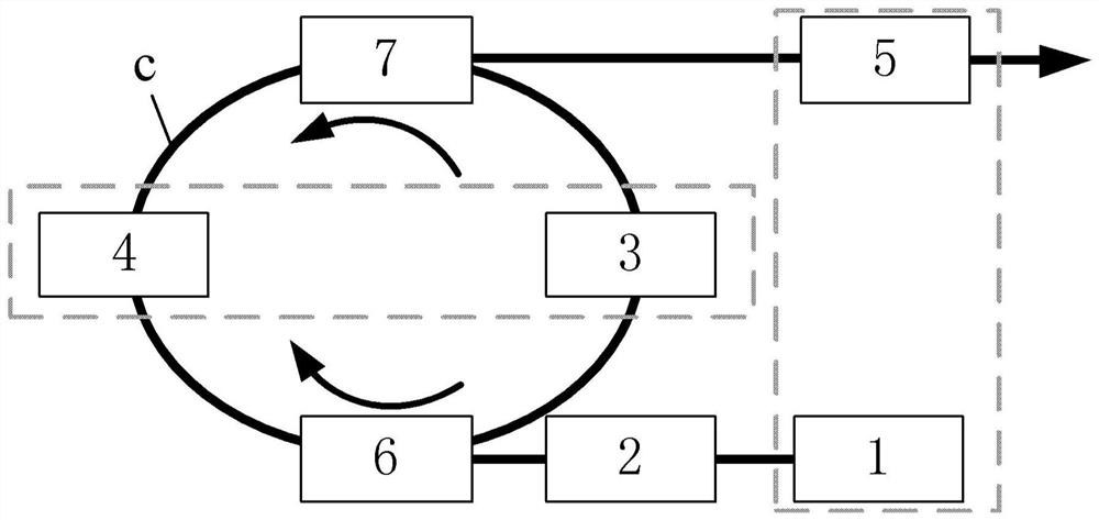
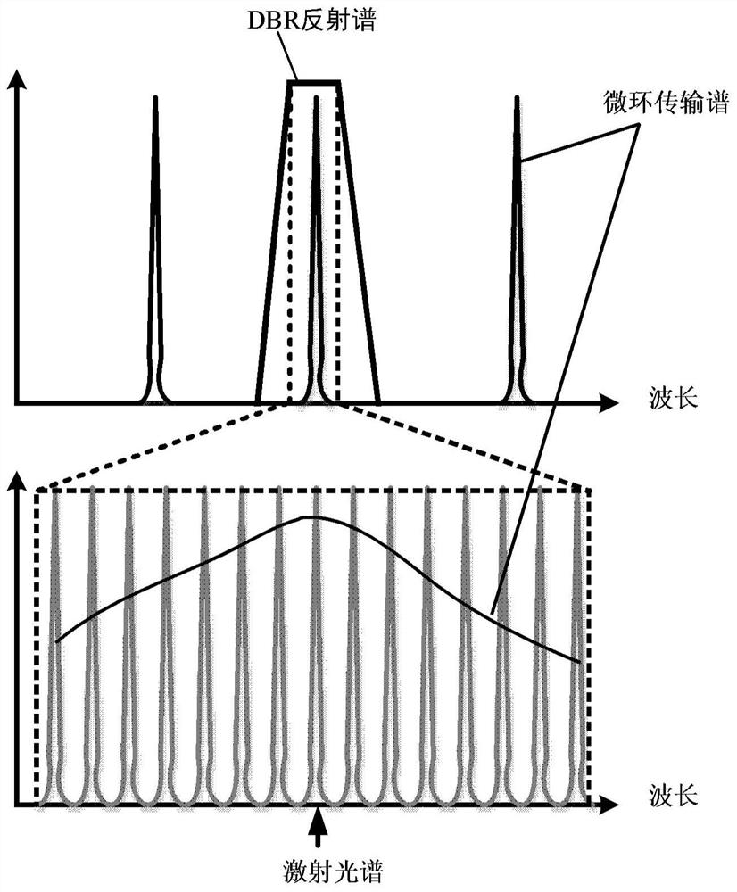
[0026] The injection current of the traditional DBR laser only passes through the passive waveguide area where the grating is located, so the change of the Bragg wavelength determined by the grating with temperature is faster than the change of the lasing ...


PUM

PropertyMeasurementUnit
wavelengthaaaaaaaaaa

Abstract

A tuned laser chip, comprising: a backward grating region (1), a first gain region (2), a microring resonator (c) and a forward grating region (5); the microring resonator (c) includes The second gain area (3), the first multi-mode interference waveguide (6), the phase modulation area (4) and the second multi-mode interference waveguide (7) which are ring-connected in sequence; the backward grating area (1) is connected to The first gain region (2), the first gain region (2) is connected to the first multimode interference waveguide (6), and the forward grating region (5) is connected to the second multimode An interference waveguide (7); wherein, the backward grating area (1) and the forward grating area (5) form a Bragg reflection resonant cavity, and the second gain area (3) and the phase modulation area (4 ) form a gain resonator. The laser chip can realize fine tuning and wide-range tuning of the L-band spectrum and avoid mode hopping.

Description

technical field [0001] The present disclosure relates to the field of optoelectronic chips, in particular to a tuned laser chip. Background technique [0002] Due to their high coherence, low frequency noise, high frequency stability and wide wavelength tuning potential, semiconductor lasers have become the core devices in the fields of ultra-high-speed optical communication, long-distance space laser communication, ultra-high-resolution lidar and optical sensing. In 100Gbps and beyond 100Gbps high-speed optical communication systems, the surge in data load has promoted the use of high-order quadrature amplitude modulation schemes such as 16-QAM and 64-QAM, which have low tolerance to phase noise and require lasers with full C-band Even full L-band tunability. [0003] Starting from practical applications, the wavelength division multiplexing (WDM) transmission system needs to consider the limitations of tunable light sources while considering the increase in bandwidth and ...

Claims


Application Information

Patent Timeline
Patent Type & Authority Patents(China)
IPC IPC(8): H01S5/10H01S5/125H01S5/14H01S5/06H01S5/065
CPCH01S5/1071H01S5/125H01S5/141H01S5/0653H01S5/0607
Inventor 孙文惠徐长达班德超陈伟祝宁华
Owner INST OF SEMICONDUCTORS - CHINESE ACAD OF SCI
Why Eureka
Try Eureka