Light-emitting diode epitaxial wafer and preparation method thereof

A technology of light-emitting diodes and epitaxial wafers, which is applied to electrical components, circuits, semiconductor devices, etc., and can solve the problems of improving the crystal quality of n-type GaN layers and p-type GaN layers

Active Publication Date: 2021-02-23
HC SEMITEK ZHEJIANG CO LTD
View PDF4 Cites 4 Cited by
  • Summary
  • Abstract
  • Description
  • Claims
  • Application Information

AI Technical Summary

Problems solved by technology

[0004] However, when the GaN buffer layer itself grows on the AlN layer, it will also accumulate some dislocation defects, and these dislocation defects will extend to structures such as the n-type GaN layer, resulting in the final n-type GaN layer, multiple quantum well layer and p The crystal quality of the GaN layer has limited improvement

Method used


Image

  • Light-emitting diode epitaxial wafer and preparation method thereof
  • Light-emitting diode epitaxial wafer and preparation method thereof
  • Light-emitting diode epitaxial wafer and preparation method thereof

Examples


Embodiment Construction

[0033] In order to make the object, technical solution and advantages of the present invention clearer, the implementation manner of the present invention will be further described in detail below in conjunction with the accompanying drawings.

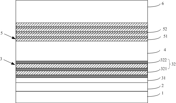
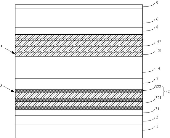
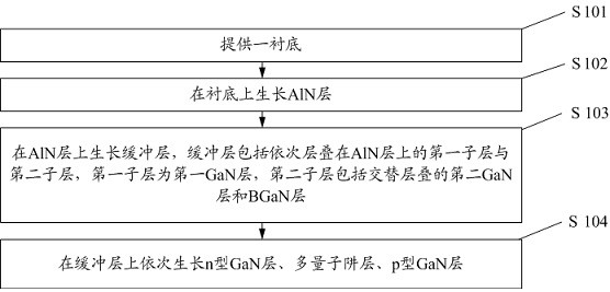
[0034] figure 1 It is a schematic structural diagram of a light-emitting diode epitaxial wafer provided by an embodiment of the present disclosure. Refer to figure 1 It can be seen that the embodiment of the present disclosure provides a light-emitting diode epitaxial wafer, which includes a substrate 1 and an AlN layer 2, a buffer layer 3, an n-type GaN layer 4, and multiple quantum wells stacked on the substrate 1 in sequence. Layer 5 and p-type GaN layer 6.

[0035] The buffer layer 3 includes a first sublayer 31 and a second sublayer 32 sequentially stacked on the AlN layer 2, the first sublayer 31 is a first GaN layer, and the second sublayer 32 includes alternately stacked second GaN layers 321 and BGaN layer 322 .

[0036] In...


PUM

PropertyMeasurementUnit
thicknessaaaaaaaaaa
thicknessaaaaaaaaaa
thicknessaaaaaaaaaa

Abstract

The invention discloses a light emitting diode epitaxial wafer and a preparation method thereof, and belongs to the field of light emitting diode manufacturing. A buffer layer comprises a first sub-layer and a second sub-layer, and the first sub-layer plays a role in transition. The second sub-layer stacked on the first sub-layer comprises second GaN layers and BGaN layers which are alternately stacked. On one hand, lattice mismatch is relieved, a good foundation is provided for growth of a subsequent epitaxial structure, and on the other hand, the BGaN layers can be inserted into or fill blank positions caused by dislocation due to the fact that the volume of B atoms is small, and defects existing in the buffer layer are reduced. Moreover, B atoms can play a certain role in positioning, so that dislocation is prevented from continuing moving into an n-type GaN layer and a multi-quantum well layer, and the crystal quality of the finally obtained light-emitting diode epitaxial wafer iseffectively improved.

Description

technical field [0001] The invention relates to the field of light-emitting diode production, in particular to a light-emitting diode epitaxial wafer and a preparation method thereof. Background technique [0002] A light emitting diode is a semiconductor electronic component that emits light. As an efficient, environmentally friendly and green new solid-state lighting source, it is being rapidly and widely used, such as traffic lights, car interior and exterior lights, urban landscape lighting, mobile phone backlight, etc. Improving the luminous efficiency of chips is the goal that LEDs are constantly pursuing. [0003] The light-emitting diode epitaxial wafer is the basic structure used to prepare light-emitting diodes. The light-emitting diode epitaxial wafer usually includes a substrate and an AlN layer, a GaN buffer layer, an n-type GaN layer, a multi-quantum well layer and a p-type GaN layer grown sequentially on the substrate. layer. The GaN buffer layer can allevia...

Claims


Application Information

Patent Timeline
Patent Type & Authority Applications(China)
IPC IPC(8): H01L33/12H01L33/06H01L33/32H01L33/14H01L33/00
CPCH01L33/0075H01L33/06H01L33/12H01L33/145H01L33/32
Inventor 洪威威王倩梅劲董彬忠
Owner HC SEMITEK ZHEJIANG CO LTD
Why Eureka
Try Eureka