Broadband terahertz wave absorber with high tolerance

A terahertz and wave absorber technology, applied in the electromagnetic field, can solve the problems of high production cost, harsh preparation environment, and high requirements for metasurfaces, and achieve the effect of low cost and good light transmission

Pending Publication Date: 2021-02-23
NANJING UNIV OF SCI & TECH
View PDF5 Cites 4 Cited by
  • Summary
  • Abstract
  • Description
  • Claims
  • Application Information

AI Technical Summary

Problems solved by technology

In addition, the metasurface structure of a terahertz absorber is often on the micron scale, with a fine structure and high requirements on the metasurface. It is usually prepared by complex processes such as photolithography and nano-transfer printing. The preparation environment is harsh and the production cost is high.

Method used


Image

  • Broadband terahertz wave absorber with high tolerance
  • Broadband terahertz wave absorber with high tolerance
  • Broadband terahertz wave absorber with high tolerance

Examples


Embodiment

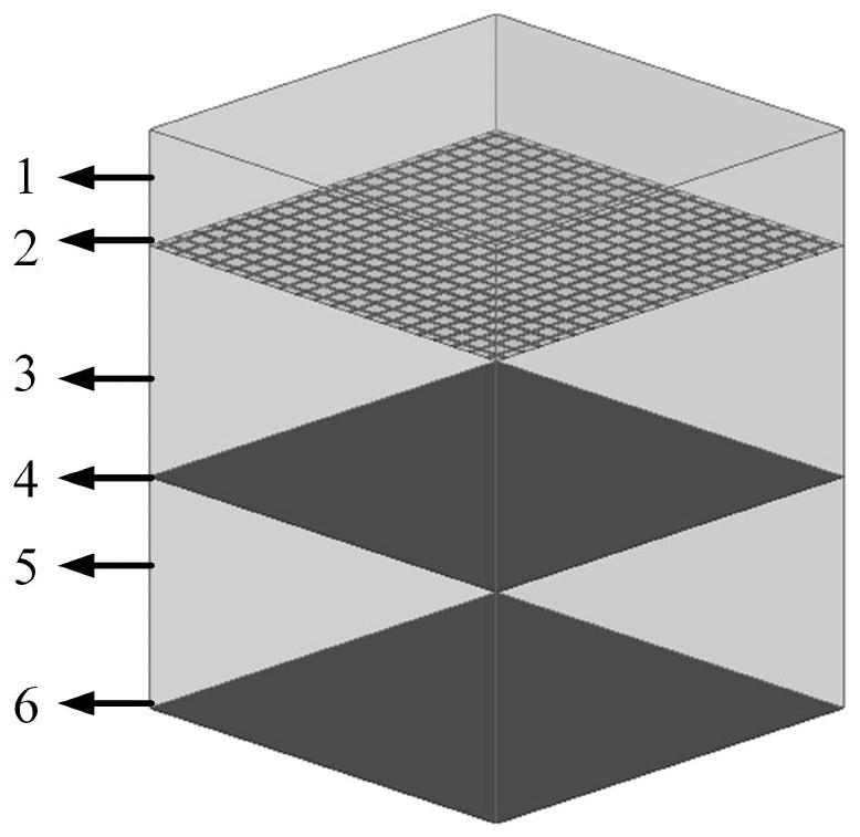
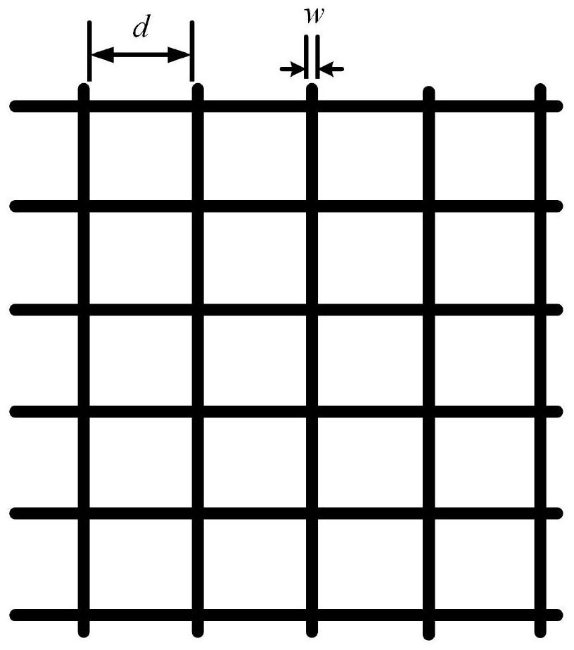
[0034] In this embodiment, CST MICROWAVE STUDIO software is used for simulation, and the protective layer, upper dielectric and lower dielectric are selected as PET, and the lossy layer and bottom plate are made of ITO material. A set of optimized parameters is shown in Table 1, where h_1 represents the thickness of the protective layer , w represents the line width of the inductive grid metasurface, d represents the spacing between two adjacent lines of the inductive grid metasurface, h_2 represents the thickness of the upper dielectric, h_3 represents the thickness of the lower dielectric, R s _1 represents the surface resistance of the inductor grid network, R s _2 represents the surface resistance of the lossy layer, R s _3 represents the surface resistance of the bottom plate.

[0035] Table 1 Specific Implementation Parameters

[0036]

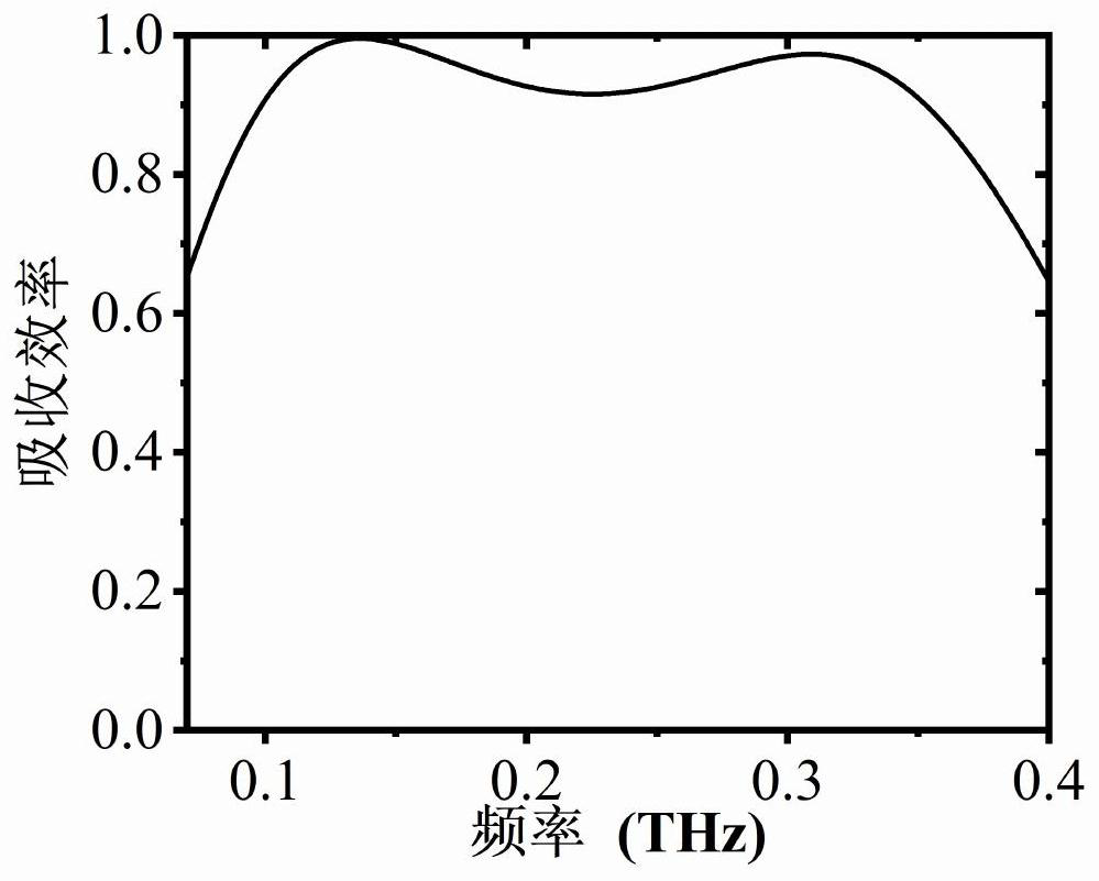
[0037] The simulated absorption efficiency curve is as follows image 3 As shown, it can be seen that the designed absorber has a...


PUM

PropertyMeasurementUnit
thicknessaaaaaaaaaa

Abstract

The invention discloses a high-tolerance broadband terahertz wave absorber which comprises a metasurface protection layer, a metasurface, an upper dielectric layer, a loss layer, a lower dielectric layer and a bottom plate from top to bottom, and is characterized in that the metasurface is printed on the lower surface of the metasurface protection layer through conductive ink. The metasurface structure is selected as an inductance grid structure, and is prepared by adopting a hyperfine electrostatic ink-jet printing technology based on an electrohydrodynamics principle. Through optimization design, the wave absorber has the advantage of high tolerance, is insensitive to the line width and the surface resistance of the metasurface, and meanwhile, keeps an ultra-wideband wave absorbing effect within a 45-degree incident range. The method has a wide application prospect in the aspects of imaging, sensing and electromagnetic stealth.

Description

technical field [0001] The invention relates to the field of electromagnetics, in particular to a high-tolerance broadband terahertz wave absorber. Background technique [0002] Terahertz technology is rated by the United States as one of the "Top Ten Technologies that Will Change the Future World", and it has broad application prospects in the fields of biomedicine, sensing technology, communication technology, and imaging. As an important terahertz device, terahertz absorber has been extensively studied. At present, most terahertz absorbers use metal materials, which are opaque in the optical band. In addition, the metasurface structure of a terahertz absorber is often on the micron scale, with a fine structure and high requirements on the metasurface. It is usually prepared by complex processes such as photolithography and nano-transfer printing. The preparation environment is harsh and the production cost is high. Contents of the invention [0003] The object of the ...

Claims


Application Information

Patent Timeline
Patent Type & Authority Applications(China)
IPC IPC(8): H01Q17/00G02B5/00
CPCH01Q17/007G02B5/003
Inventor 顾文华王俊杰吴杨慧傅晨陈雪
Owner NANJING UNIV OF SCI & TECH
Why Eureka
Try Eureka