
Resistive random access memory and manufacturing method thereof

A technology of resistive variable memory and manufacturing method, which is applied in the direction of electrical components, etc., can solve the problems of randomness in formation and fracture, and affect the working stability and reliability of resistive variable memory, so as to improve the working stability and reliability, increase Concentration, Consistency-enhancing Effects

Pending Publication Date: 2021-02-26
SHANGHAI HUALI MICROELECTRONICS CORP
View PDF0 Cites 2 Cited by
  • Summary
  • Abstract
  • Description
  • Claims
  • Application Information

AI Technical Summary

Problems solved by technology

[0005] The purpose of the present invention is to provide a resistive memory and its preparation method to solve the problem that the formation and breakage of the conductive channel of the resistive memory is random and affect the working stability and reliability of the resistive memory

Method used


Image

  • Resistive random access memory and manufacturing method thereof
  • Resistive random access memory and manufacturing method thereof
  • Resistive random access memory and manufacturing method thereof

Examples


Embodiment Construction

[0029] The resistive memory and its manufacturing method proposed by the present invention will be further described in detail below with reference to the accompanying drawings and specific embodiments. The advantages and features of the present invention will become clearer from the following description. It should be noted that all the drawings are in a very simplified form and use imprecise scales, and are only used to facilitate and clearly assist the purpose of illustrating the embodiments of the present invention.

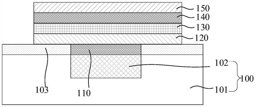
[0030] Please refer to figure 1 , which is a schematic structural diagram of the resistive memory provided by the present invention. like figure 1 As shown, the present invention provides a resistive variable memory, including: a semiconductor substrate 100 , a first electrode 110 , a first intercalation layer 120 , a resistive variable layer 130 , a second intercalation layer 140 and the second electrode 150 .

[0031] Specifically, the RRAM further inclu...


PUM

PropertyMeasurementUnit
thicknessaaaaaaaaaa
thicknessaaaaaaaaaa
thicknessaaaaaaaaaa

Abstract

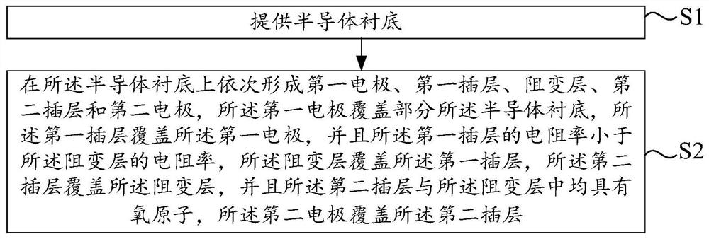
The invention provides a resistive random access memory and a manufacturing method thereof. The resistive random access memory comprises a semiconductor substrate, a first electrode, a first intercalation layer, a resistive random access layer, a second intercalation layer and a second electrode, the first electrode covers a part of the semiconductor substrate, the first intercalation layer coversthe first electrode, a resistance of the first intercalation layer is smaller than that of the resistive random access layer, the resistive random access layer covers the first intercalation layer, the second intercalation layer covers the resistive random access layer, oxygen atoms exist in the second intercalation layer and the resistive random access layer, and the second electrode covers thesecond intercalation layer. Due to the fact that oxygen atoms exist in the second intercalation layer and the resistive random access layer, after the resistive random access memory applies a positivevoltage, the oxygen atoms in the resistive random access layer and the second intercalation layer can move towards the second electrode, the concentration of oxygen vacancies can be increased, generation of oxygen vacancy conductive filaments is facilitated, and the consistency of the resistive random access memory is further improved.

Description

technical field [0001] The invention relates to the field of semiconductor integrated circuit manufacturing, in particular to a resistive variable memory and a manufacturing method thereof. Background technique [0002] With the development of semiconductor technology, the market demand for non-volatile memory is increasingly shifting towards large capacity, low power consumption, high density and low cost. Resistive Random Access Memory (RRAM) is a research hotspot of next-generation memory, has strong application potential, and is considered to be the memory with the most commercial value. [0003] In the existing resistive variable memory, it generally includes: a semiconductor substrate, a bottom electrode, a resistive layer and a top electrode, the bottom electrode covers the semiconductor substrate, the resistive layer covers the bottom electrode, the A top electrode covers the resistive switch layer. Wherein, the resistive switch layer has oxygen atoms. In the resi...

Claims


Application Information

Patent Timeline
Patent Type & Authority Applications(China)
IPC IPC(8): H01L45/00
CPCH10N70/24H10N70/801H10N70/011H10N70/8833
Inventor 田伟思邹荣王奇伟陈昊瑜
Owner SHANGHAI HUALI MICROELECTRONICS CORP
Learn More