

Automatic adhesive tape packaging method for FOSB assembly line
A packaging method and assembly line technology, which can be used in packaging, conveyor belt wrapping, and rotating wrapping of items, etc., can solve the problems of low degree of automation, high work efficiency, and difficulty in finding tape heads.
- Summary
- Abstract
- Description
- Claims
- Application Information
AI Technical Summary
Problems solved by technology
Method used
Image

Examples
Embodiment Construction
[0057] The present invention will be further described below in conjunction with accompanying drawing:
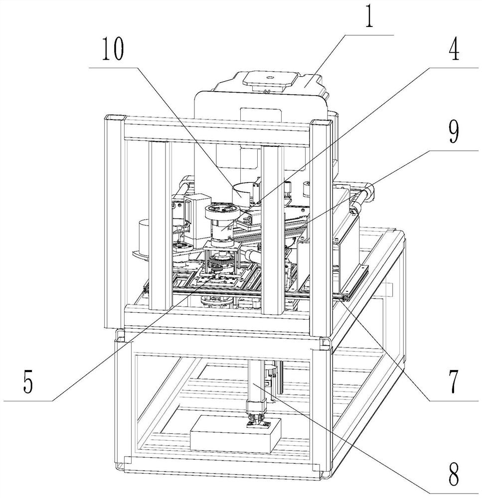
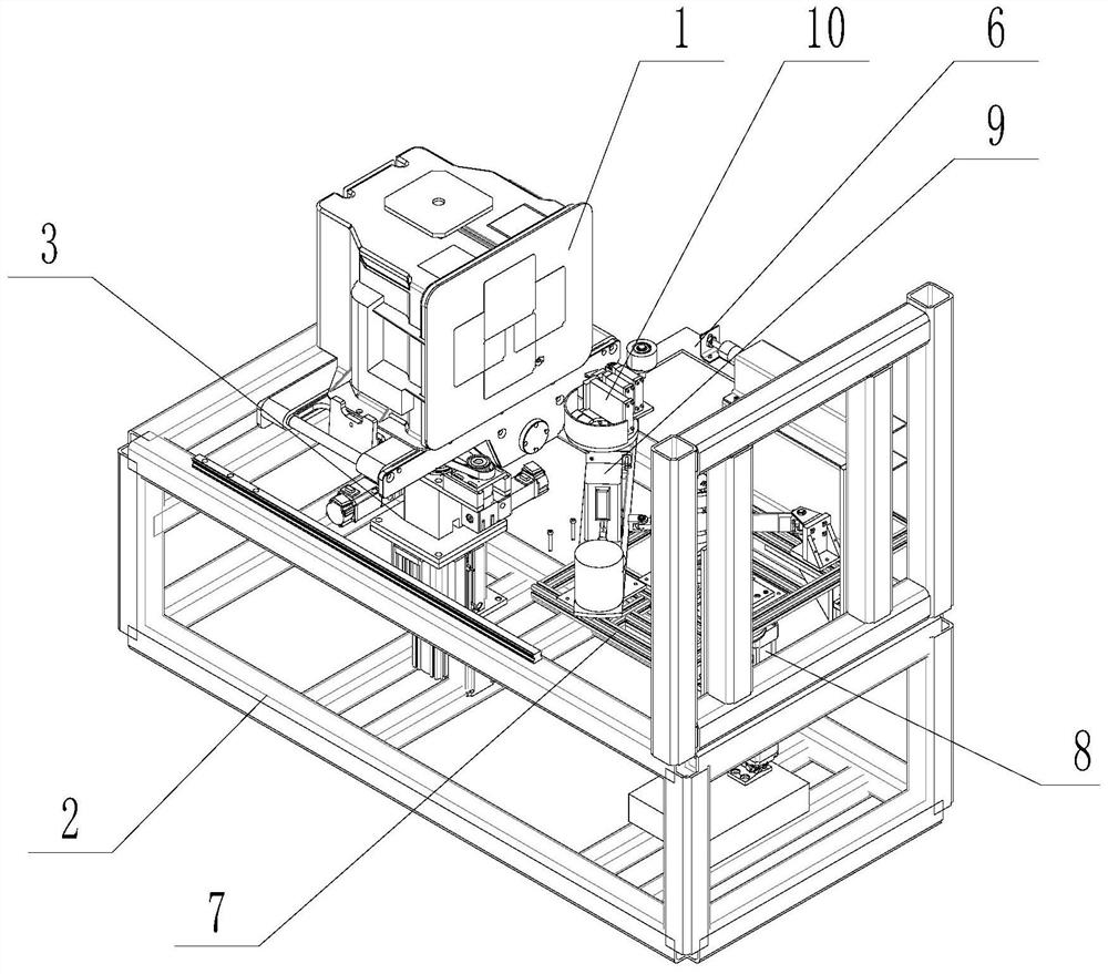
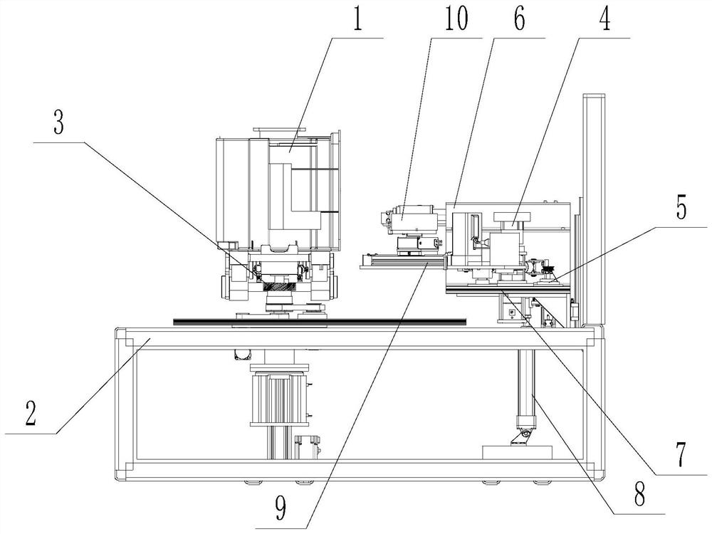
[0058] Such as Figure 1-13 Shown, a kind of automatic adhesive tape packaging method of FOSB assembly line, specifically comprises the following steps:
[0059] Step 1: Fix the wafer packaging box 1 on the workpiece support rotary transmission device 3 that can drive the wafer packaging box 1 to rotate, and at the same time fix the tape with the tape head on the tape fixing device 4 through the pneumatic three-jaw chuck 41 , the tape rotating drive device 5 is connected to the tape fixing device 4 and drives the pneumatic three-jaw chuck 41 on the tape fixing device 4 to rotate together with the tape, so that the tape head rotates with the tape;
[0060] Step 2: Utilize the cantilever rotating cylinder 95 to drive the cantilever device 9 to rotate close to the tape fixing device 4, and the cantilever linear module 94 on the cantilever device 9 drives the tape taking head ...
PUM
 Abstract
Description
Claims
Application Information