Method for etching cantilever beam on CSOI

A cantilever beam and insulating layer technology, which is applied in the field of semiconductor manufacturing technology, can solve the problems of device yield reduction, upper surface layer depression, etch damage, and achieve the effect of improving yield

Pending Publication Date: 2021-03-02
武汉敏声新技术有限公司
View PDF0 Cites 0 Cited by
  • Summary
  • Abstract
  • Description
  • Claims
  • Application Information

AI Technical Summary

Problems solved by technology

However, in the process of device fabrication, due to the low pressure inside the cavity, a large pressure difference is formed between the external environment and the cavity, and the upper surface of the CSOI will be under the pressure brought by atmospheric pressure, resulting in the upper surface The layer is depressed inward, followed by unevenness in the material layer deposited on the CSOI
Secondly, when etching a cantilever beam in a structure with a cavity, there will be a problem of local damage at the etching site due to the pressure difference between the inside and outside, which will lead to a decrease in the yield of the device

Method used


Image

  • Method for etching cantilever beam on CSOI
  • Method for etching cantilever beam on CSOI
  • Method for etching cantilever beam on CSOI

Examples


Embodiment 1

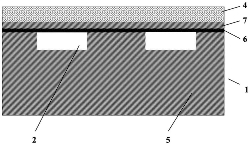
[0033]Such asFigure 1-5 As shown, a method for etching a cantilever beam on CSOI includes the following steps:

[0034]Step 1: Provide a set of silicon wafers as the first insulating layer 5, and fabricate a cavity 2 structure on the surface of the first insulating layer 5;

[0035]Step 2: Bonding a composite layer composed of a transition layer 6 and a second insulating layer 7 on the surface of the first insulating layer 5 to form a wafer substrate 1 together;

[0036]Step 3: Depositing materials sequentially on the surface of the composite layer to form the structural layer 4;

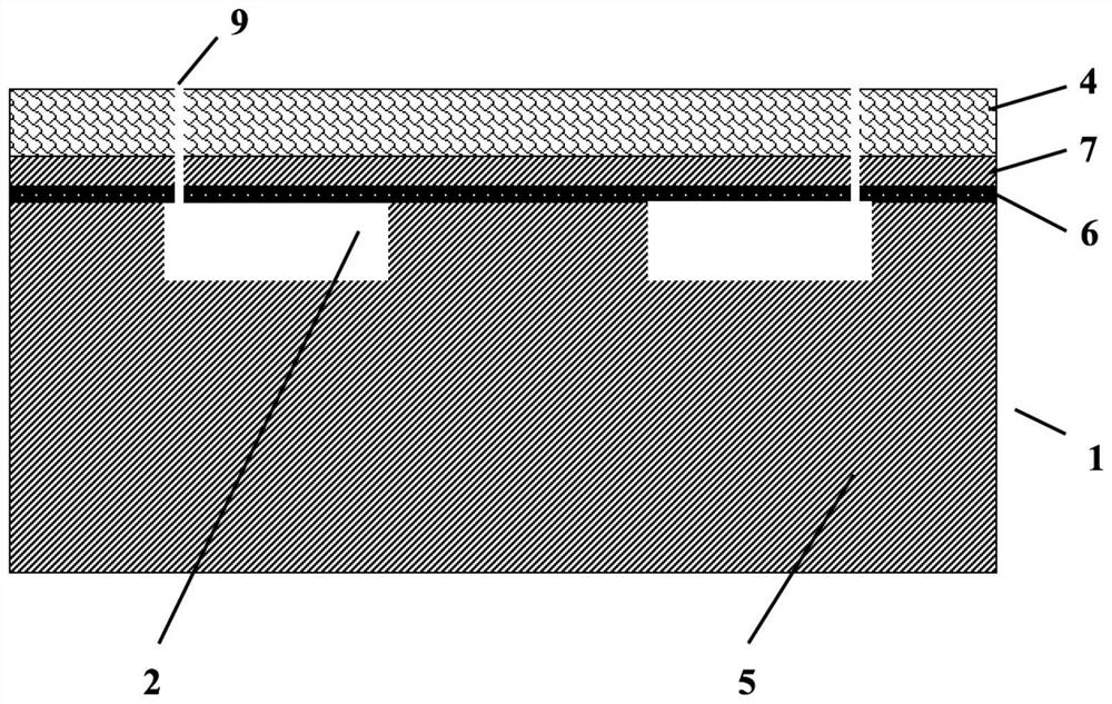
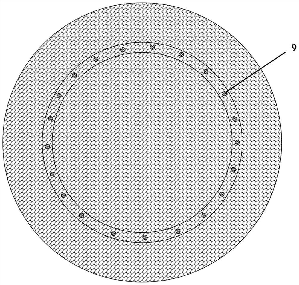
[0037]Step 4: Etch the structure layer 4, the second insulating layer 7 and the transition layer 6 anywhere within the target etching area 3 from top to bottom to form a plurality of vent holes 9 so that the outside world is connected to the cavity 2;

[0038]Step 5: Perform pattern etching on the original target etching area 3, and finally form a target structure.

[0039]In other embodiments, the first insulating layer 5...

Embodiment 2

[0044]Such asFigure 1-6As shown, the difference between this embodiment and Embodiment 1 lies in:

[0045]The step 1 further includes the following operations: filling the cavity 2 with silicon dioxide 8 to keep the surface of the first insulating layer 5 even.

[0046]The silicon substrate surface of the first insulating layer 5 is flattened by pre-embedded silicon dioxide 8, and after bonding the composite layer, a flat first insulating layer 5 / transition layer 6 / second insulating layer 7 substrate is formed, which is next to the flat The material is deposited uniformly on the surface of the structure layer 4 to maintain the flatness, and the actual processed device can restore the ideal situation to the greatest extent. The embedded silicon dioxide 8 is released during etching.


PUM


Abstract

The invention relates to a semiconductor manufacturing process, in particular to a method for etching a cantilever beam on a CSOI, which comprises the following steps: providing a group of silicon wafers as a first insulating layer, and manufacturing a cavity structure on the surface of the first insulating layer; bonding a composite layer composed of a transition layer and a second insulating layer on the surface of the first insulating layer; sequentially depositing materials on the surface of the composite layer to form a structural layer; etching the structural layer, the second insulatinglayer and the transition layer from top to bottom at any place in the range of the target etching region to form a plurality of vent holes so that the outside is connected with the cavity; and carrying out patterned etching on the original target etching region, and finally forming a target structure. According to the method, the small vent holes are etched in the target etching range of the structural layer of the CSOI to eliminate the pressure difference formed between the internal vacuum cavity and the external atmospheric pressure, and then predetermined etching is performed, so that thecantilever beam cannot be locally damaged due to overlarge internal and external pressure difference in the etching process, and the yield of the device is improved.

Description

Technical field[0001]The invention relates to a semiconductor manufacturing process, in particular to a method for etching a cantilever beam on a CSOI.Background technique[0002]CSOI, the full name of Cavity Silicon-On-insulator, is silicon on an insulating substrate with a cavity. The target structure can be formed by depositing corresponding materials on CSOI. For example, an ultrasonic transducer can be fabricated on a substrate with a cavity. Achieve specific functions. However, in the process of device manufacturing, due to the low pressure inside the cavity, a large pressure difference is formed between the external environment and the cavity. The upper surface of the CSOI will be subjected to the pressure brought by the atmospheric pressure, resulting in the upper surface The layer is compressed to the inside, and the material layer deposited on the CSOI will appear uneven. Secondly, etching the cantilever beam in a structure with a cavity will cause local damage at the etched...

Claims


Application Information

Patent Timeline
Patent Type & Authority Applications(China)
IPC IPC(8): H01L21/304B81B7/00B81C1/00
CPCB81B7/0009B81C1/0015H01L21/304
Inventor 孙成亮林炳辉胡博豪吴志鹏
Owner 武汉敏声新技术有限公司
Why Eureka
Try Eureka