Light emitting diode and manufacturing method thereof

A technology for light-emitting diodes and a manufacturing method, which is applied to semiconductor devices, electrical components, circuits, etc., can solve the problems of difficulty in forming a patterned mask on the side of the light-emitting diode, pattern transfer that cannot be masked, etc. The effect of dissipating heat and increasing the contact area

Active Publication Date: 2021-03-05
ANHUI SANAN OPTOELECTRONICS CO LTD
View PDF4 Cites 6 Cited by
  • Summary
  • Abstract
  • Description
  • Claims
  • Application Information

AI Technical Summary

Problems solved by technology

Usually, the surface of the light-emitting diode is coated with a photoresist mask layer, and the surface is roughened through exposure, development and etching processes. However, in the conventional exposure process, the exposure beam is vertically incident on the upper surface of the light-emitting diode, and its side cannot be or effectively exposed. The irradiation of the light beam makes it difficult to form an effective patterned mask on the side of the LED, so that the pattern of the mask cannot be transferred to the side of the LED for roughening treatment

Method used


Image

  • Light emitting diode and manufacturing method thereof
  • Light emitting diode and manufacturing method thereof
  • Light emitting diode and manufacturing method thereof

Examples


Embodiment 1

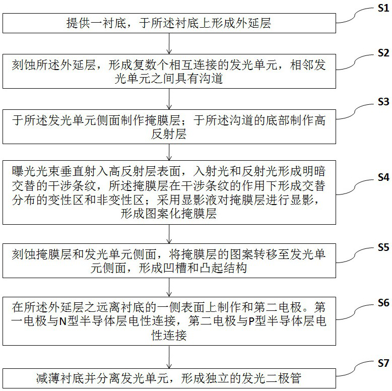
[0042] attached figure 1 It is a flow chart of the light-emitting diode manufacturing method in Embodiment 1 of the present invention. See attached figure 1 , the present invention provides a light-emitting diode manufacturing method using the interference fringes of the exposure beam to expose the side of the light-emitting diode to form grooves and raised structures, which includes:

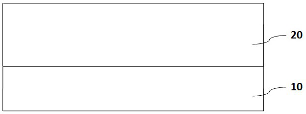
[0043] S1, see attached figure 2 , a substrate 10 is provided, and an epitaxial layer 20 is formed on the substrate 10 .

[0044]Wherein, the material of the substrate 10 is selected from Al2O3, SiC, GaAs, GaN, AlN, GaP, Si, ZnO, MnO and any combination thereof. The epitaxial growth substrate 10 of this embodiment is illustrated by taking a sapphire substrate 10 (sapphire substrate) as an example, and the lattice direction is (0001), for example, but the present invention does not limit the material and lattice direction of the substrate 10 used. The substrate 10 can be patterned to change...

Embodiment 2

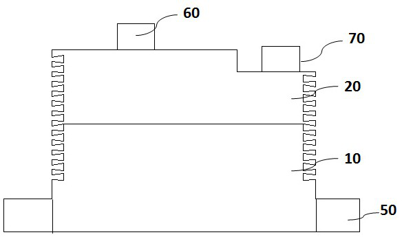
[0068] attached Figure 8 A schematic diagram of the structure of the light emitting diode of the present invention is shown. The light-emitting diode disclosed in the present invention is manufactured by the method of the above-mentioned embodiment 1. The details are as follows: a light-emitting diode, including a substrate 10 and an epitaxial layer 20 stacked on the substrate 10, the side of the epitaxial layer 20 has a groove 82 and a protrusion 81 structure, and the width of the bottom of the groove 82 is greater than the width of the opening .

[0069] The structure of grooves 82 and protrusions 81 on the side of the epitaxial layer 20, on the one hand, changes the path of light incident on the side of the light-emitting diode, which is more conducive to light output, and on the other hand, increases the contact area between the epitaxial layer 20 and the surrounding medium , is conducive to heat dissipation.

[0070] See attached Figure 9 , in this embodiment, the p...


PUM

PropertyMeasurementUnit
wavelengthaaaaaaaaaa
sizeaaaaaaaaaa
heightaaaaaaaaaa

Abstract

The invention belongs to the field of semiconductors, and particularly relates to a light emitting diode and a manufacturing method thereof. A channel is etched between adjacent light emitting units,a high-reflection layer is manufactured at the bottom of the channel, interference fringes are generated through the high-reflection layer, and the side surface of the light emitting diode is exposedby adopting the interference fringes; therefore, the groove and the protruding structure are formed on the side face of the light-emitting diode, the width of the bottom of the groove is larger than that of the opening, the silicon dioxide layer is arranged on the surface of the protruding structure, and light-emitting efficiency of the light-emitting diode can be further improved.

Description

technical field [0001] The invention belongs to the field of semiconductor manufacturing, and in particular relates to a light emitting diode and a manufacturing method thereof. Background technique [0002] The light emitting diode structure in the prior art generally includes a substrate, an epitaxial layer disposed on the substrate, and electrodes located on the epitaxial layer. With the popularity of light-emitting diodes as lighting devices, improving their luminous efficiency has become an increasingly important technical difficulty. Luminous efficiency can be improved by increasing internal quantum efficiency or external quantum efficiency. Roughening the surface of light-emitting diodes has become a conventional process for improving the external quantum efficiency of light-emitting diodes. Usually, the surface of the light-emitting diode is coated with a photoresist mask layer, and the surface is roughened through exposure, development and etching processes. Howev...

Claims


Application Information

Patent Timeline
Patent Type & Authority Applications(China)
IPC IPC(8): H01L33/22H01L33/46H01L27/15
CPCH01L27/156H01L33/46H01L33/22H01L33/20H01L2933/0008H01L2933/0083H01L2933/0025H01L33/0095H01L33/10H01L33/56H01L33/0054H01L33/02
Inventor 毕东升徐凯蔡家豪黄照明张家豪
Owner ANHUI SANAN OPTOELECTRONICS CO LTD
Why Eureka
Try Eureka