

Full-color SMD LED with enhanced waterproof performance
A LED chip and performance technology, applied in the direction of instruments, electrical components, electric solid devices, etc., can solve the problems of double-electrode chip electrode metal migration failure, colloid and substrate delamination, silver colloid delamination failure, etc., to achieve air tightness Good, the degree of delamination is reduced, and the effect of reducing production costs
- Summary
- Abstract
- Description
- Claims
- Application Information
AI Technical Summary
Problems solved by technology
Method used
Image

Examples
Embodiment 1
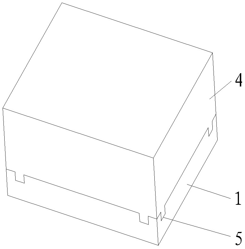
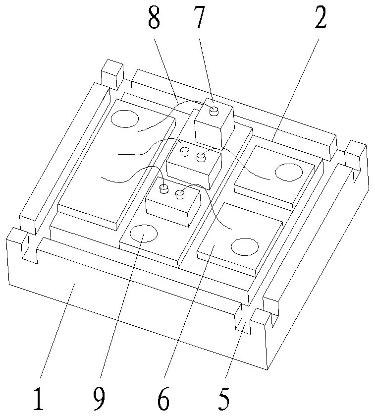
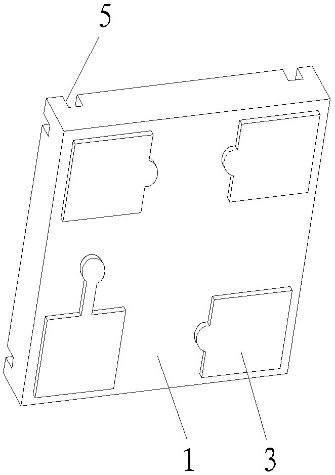
[0015] Such as Figure 1 to 3 As shown, a full-color SMD LED that enhances waterproof performance includes a substrate 1, and is provided on the LED function zone 2 on the upper surface of the substrate 1, and the electrode 3 is provided on the lower surface of the substrate 1, and the package colloid 4 is provided on the substrate 1. The substrate 1 is located at the upper surface of the LED functional region 2, and the waterproof groove 5 is provided, the waterproof groove 5 is a concave tank structure, which is lower than the LED function zone 2, so the functional zone is equivalent to a boss, and when the mold is packaged. The glue is combined with three faces of each groove, and the encapsulation colloid 4 is embedded in the waterproof groove 5 to form a waterproof structure, effectively preventing moisture from directly entering the row from the lamp beads directly into the functional region. The substrate 1 is provided with a through hole of the LED function zone 2, the elec...
Embodiment 2
[0017] Such as Figure 1 to 3 As shown, a full-color SMD LED, which enhances waterproof performance, as in the example, the only difference is that the blind hole 9 does not plug the hole treatment, and the encapsulation colloid is injected through the front of the hole, and finally fill the entire blind. Hole 9.
[0018] The type of lamp beads used in the present invention includes a single separation device, a plurality of integrated devices.
[0019] The process steps of the present invention are as follows:
[0020] Step 1: The substrate 1 is processed;
[0021] Step 2: Substrate 1 plasma cleaning treatment;
[0022] Step 3: Substrate 1 solid crystal, welding wire or flip chip solid crystal;
[0023] Step 4: Sprinkling or vacuum coating is performed on the surface of the semi-finished LED functional region 2 using the Presin Gabani inorganic material mixture coating. The film layer of spray or vacuum vapor deposition is first cured, and the film layer after curing is optical tr...
PUM
 Abstract
Description
Claims
Application Information