Graphene-based optical carrier microwave antenna

An optical carrier microwave and graphene technology, which is applied to antennas, resonant antennas, antenna parts and other directions, can solve the problems of low optical signal conversion efficiency, high cost and complex structure of optical carrier microwave antennas, and achieves high speed and size. Small, simple hardware structure

Active Publication Date: 2021-03-12
YANGTZE NORMAL UNIVERSITY
View PDF6 Cites 2 Cited by
  • Summary
  • Abstract
  • Description
  • Claims
  • Application Information

AI Technical Summary

Problems solved by technology

[0005] In view of the above-mentioned deficiencies in the prior art, the purpose of the present invention is to provide a graphene-based light-borne microwave antenna to solve the problems of low optical signal conversion efficiency, complex structure and high cost of existing light-borne microwave antennas.

Method used


Image

  • Graphene-based optical carrier microwave antenna
  • Graphene-based optical carrier microwave antenna
  • Graphene-based optical carrier microwave antenna

Examples


Embodiment 1

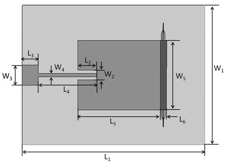
[0036] A graphene-based light-borne microwave antenna, the basic dimensions (unit: mm) are as follows:

[0037] That

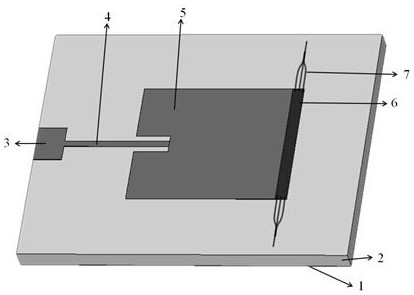
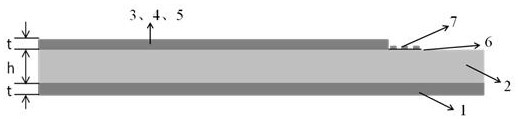
[0038] Among them, the optical waveguide 7 has a height of 200nm and a width of 400nm. The material of the insulating dielectric substrate 2 of the microstrip patch antenna is FR-4 with a thickness of 1.5mm, wherein the relative dielectric constant is 4.3, and the loss tangent value is 0.025; the metal ground plate 1, the microstrip connecting line 3, and the impedance matching Both the transmission line 5 and the radiation patch 5 are made of copper; the feed structure of the microstrip line of the antenna adopts a side feed mode, and the input impedance is 50 ohms, which realizes impedance matching well.

[0039] see Figure 4, is the simulation result graph of the input reflection coefficient S11 under different graphene Fermi levels (corresponding to different optical signal intensities) of the present invention. The operating frequency of the graphen...

Embodiment 2-5

[0041] The basic dimensions (unit: mm) are as follows:

[0042] Example L 1* W 1

L 2* W 2

L 3* W 3

L 4* W 4

L 5* W 5

L 6* W 5

t h Example 2 31.2*28 2.5*1 2.5*1.9 9.5*0.5 14.2*11.8 05*11.8 0.018 0.06 Example 3 30.7*20 3.5*1 2.5*1.9 10*0.6 10*10 1*10 0.018 1 Example 4 27.7*22 3.5*2 2.8*2.9 9*0.65 14*18 1.5*18 0.035 1.5 Example 5 26.5*22 3.2*1.4 3.5*3.5 8.5*0.48 15.6*13.8 1.2*13.8 0.026 2

[0043] Example The size range of optical waveguide is (100~400)×(400~2000) Example 2 400×2000 Example 3 100×400 Example 4 280×1000 Example 5 300×1600

[0044] The unit of size is nm. The operating frequency of the graphene optical microwave antenna in this implementation is 3.5-6 GHz.

[0045] Wherein, the metal ground plate 1 and the metal structure layer (microstrip connection line 3, impedance matching transmission line 4 and radiation ...


PUM

PropertyMeasurementUnit
Thicknessaaaaaaaaaa

Abstract

The invention provides a graphene-based optical carrier microwave antenna, which is composed of a metal grounding plate, an insulating dielectric layer, a metal structure layer, a graphene film patchand an optical waveguide. The metal structure layer comprises a microstrip connecting line, an impedance matching transmission line and a radiation patch. According to the antenna, when signal light irradiates the graphene patch, the conductivity of graphene is changed along with the intensity of the signal light, so that an optical signal is converted into a microwave radiation signal. Accordingto the antenna, the optical adjustability of the graphene is utilized, the high electron mobility of the graphene and the resonance property of the metal antenna structure are combined, optical signals can be directly converted into microwave signals without photoelectric signal conversion, the hardware structure is simple, the speed is high, the size is small, and the antenna can be applied to high-speed wireless communication.

Description

technical field [0001] The invention relates to the technical field of microwave antennas, in particular to a graphene-based light-borne microwave antenna. Background technique [0002] The antenna is the only device in the entire communication system that has a coupling relationship with the surrounding environment. Wireless communication is suitable for information transmission between the base station and the terminal. It usually converts the electrical signal in the transmission line into electromagnetic waves radiated in space, or converts electromagnetic waves in space. Converted to an electrical signal in a transmission line. The development speed of 5G and other mobile communication technologies has far exceeded people's expectations. Optical communication is suitable for long-distance information transmission. Converting optical signals into wireless microwave signals is a necessary step in communication technology. [0003] The process of converting traditional op...

Claims


Application Information

Patent Timeline
IPC IPC(8): H01Q1/36H01Q1/38H01Q5/28H01Q5/307H01Q9/04
CPCH01Q1/368H01Q1/38H01Q9/0407H01Q5/28H01Q5/307Y02D30/70
Inventor 夏良平曾梦婷张满涂红党随虎杜春雷
Owner YANGTZE NORMAL UNIVERSITY
Why Eureka
Try Eureka