Insulated gate bipolar transistor and preparation method thereof

A technology of bipolar transistors and insulated gates, which is applied in the direction of transistors, semiconductor/solid-state device manufacturing, semiconductor devices, etc., can solve the problems of poor robustness and high conduction voltage, so as to improve the robustness, improve the distribution of carriers, reduce the The effect of small parasitic resistance

Pending Publication Date: 2021-03-16
GLOBAL ENERGY INTERCONNECTION RES INST CO LTD +3
View PDF0 Cites 1 Cited by
  • Summary
  • Abstract
  • Description
  • Claims
  • Application Information

AI Technical Summary

Problems solved by technology

[0004] In order to overcome the shortcomings of high conduction voltage and poor robustness in the above-mentioned prior art, the present invention provides an insulated gate bipolar transistor, comprising an N-drift region (4), a P-type base region (5), an N-buffer layer ( 10) and N+ emission area (6);

Method used


Image

  • Insulated gate bipolar transistor and preparation method thereof
  • Insulated gate bipolar transistor and preparation method thereof
  • Insulated gate bipolar transistor and preparation method thereof

Examples


Embodiment 1

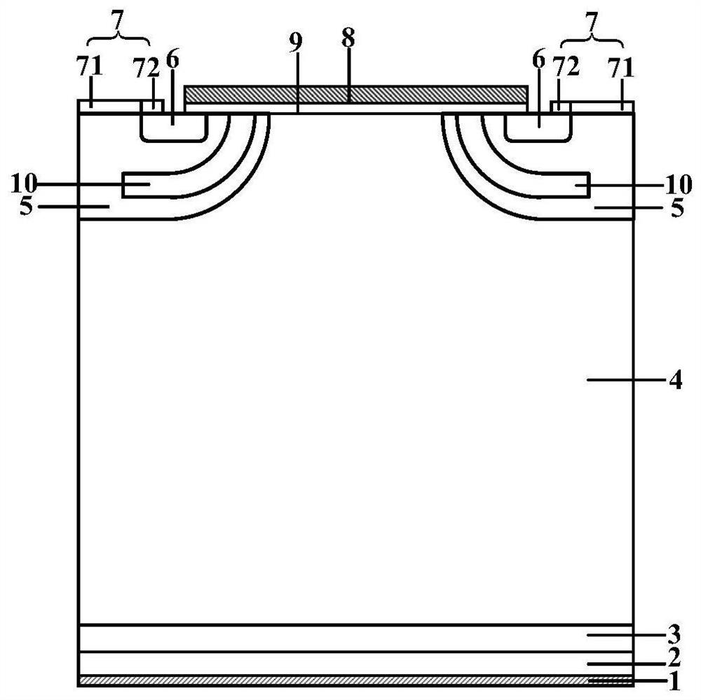
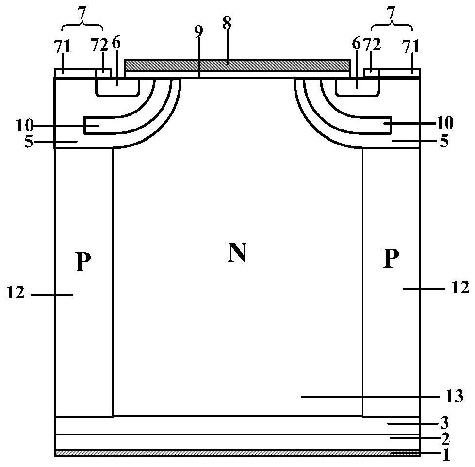
[0061] Embodiment 1 of the present invention provides an insulated gate bipolar transistor, such as figure 1 As shown, it includes N-drift region (4), P-type base region (5), N-buffer layer (10), N+ emission region (6);

[0062] The P-type base region (5) is located on both sides of the upper surface of the N-drift region (4), and the N+ emitter region (6) is located on the upper surface of the P-type base region (5), and is separated from the P-type base region (5). ) has a set distance outside; the N-buffer layer (10) (that is, the N-type charge storage layer) is located inside the P-type base region (5) below the N+ emitter region (6).

[0063] The distance between the outside of the N-buffer layer (10) and the edge of the N-drift region (4) is smaller than the distance between the outside of the N+ emitting region (6) and the edge of the N-drift region (4).

[0064] The middle position on the upper surface of the N-drift region (4) also includes: a grid (8) and a gate die...
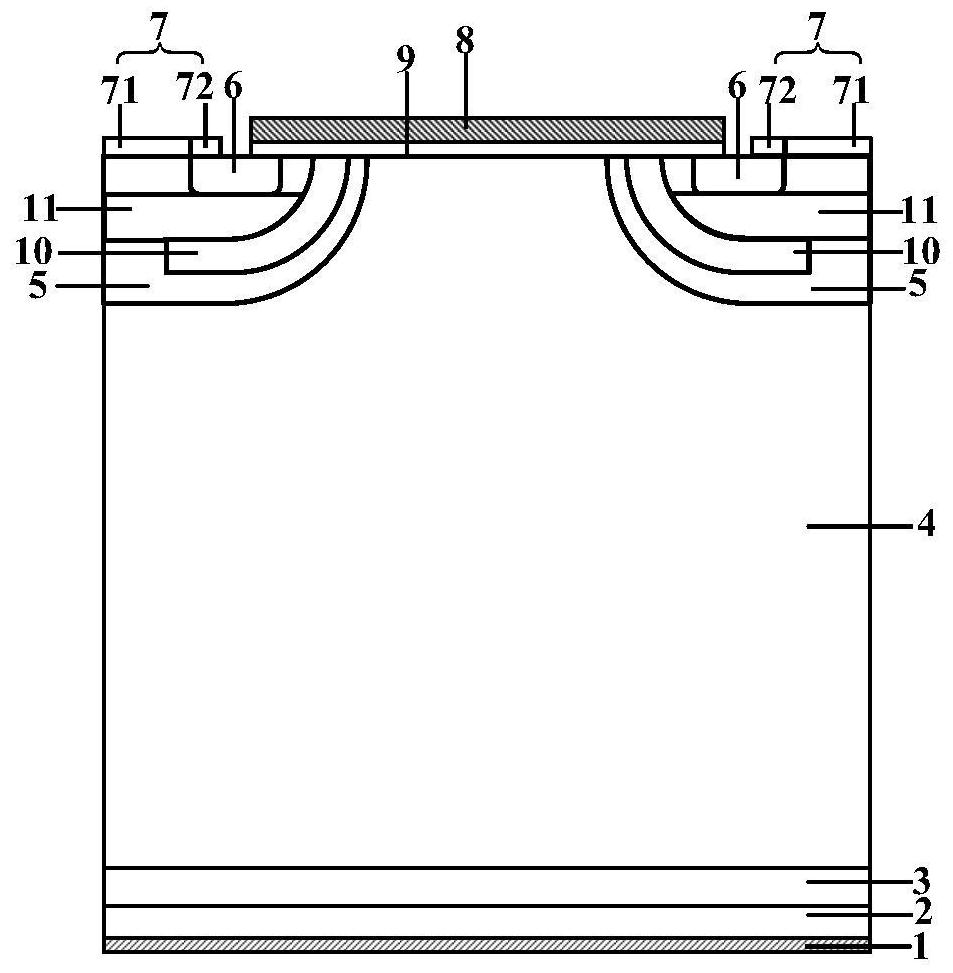
Embodiment 2

[0097] Embodiment 2 of the present invention provides a method for preparing an insulated gate bipolar transistor, the specific flow chart is shown in the figure, and the specific process is as follows:

[0098] S101: forming a P-type base region (5) on both sides of the upper surface of the N-drift region (4);

[0099] S102: forming an N-buffer layer (10) inside the P-type base region (5);

[0100] S103: forming an N+ emitter region (6) on the upper surface of the P-type base region (5) above the N-buffer layer (10) and having a set distance from the outside of the P-type base region (5).

[0101] In the above S101, a P-type base region (5) is formed on both sides of the upper surface of the N-drift region (4), including:

[0102] A P-type base region (5) is formed on both sides of the upper surface of the N-drift region (4) by sequentially adopting a thermal oxidation process, a glue coating process, a photolithography process, an ion implantation process and an annealing p...


PUM

PropertyMeasurementUnit
thicknessaaaaaaaaaa
widthaaaaaaaaaa
thicknessaaaaaaaaaa

Abstract

The invention provides an insulated gate bipolar transistor and a preparation method thereof. The insulated gate bipolar transistor comprises an N-drift region (4), P-type base regions (5), N-buffer layers (10) and N+emitter regions (6); the P-type base regions (5) are located on the two sides of the upper surface of the N-drift region (4), and the N+emitter regions (6) are located on the upper surfaces of the P-type base regions (5) and have a set distance away from the outer sides of the P-type base regions (5); and the N-buffer layers (10) are located in the P-type base regions (5) below the N+emitter regions (6), the conduction voltage drop of the insulated gate bipolar transistor is reduced through the N-buffer layers (10), and the latch-up phenomenon of the insulated gate bipolar transistor is effectively inhibited. According to the insulated gate bipolar transistor, the carrier concentration in the drift region is improved through Schottky contact, and the distribution of carriers in the drift region of the insulated gate bipolar transistor is further improved, so that the conductivity modulation effect is enhanced, the conduction voltage drop is reduced, the firmness of theinsulated gate bipolar transistor is improved through the N-buffer layers, and the large-current turn-off capability of the insulated gate bipolar transistor is improved.

Description

technical field [0001] The invention relates to the technical field of semiconductors, in particular to an insulated gate bipolar transistor and a preparation method thereof. Background technique [0002] Power semiconductor devices, as the core components in power electronic systems, have always been indispensable and important electronic components. Insulated gate bipolar transistor (IGBT) is an improved power device that can replace bipolar junction power transistors. As a new generation of power electronic devices, IGBT combines the advantages of field effect transistor (MOSFET) and bipolar crystal transistor (BJT), which not only has the advantages of easy driving of MOSFET, low input impedance and fast switching speed, but also has the advantages of Due to the advantages of high state current density, low conduction voltage, low loss and good stability, it has developed into one of the core electronic components in modern power electronic circuits and is widely used i...

Claims


Application Information

Patent Timeline
Patent Type & Authority Applications(China)
IPC IPC(8): H01L29/06H01L29/10H01L29/47H01L29/739H01L21/331
CPCH01L29/0623H01L29/0684H01L29/1004H01L29/47H01L29/66333H01L29/7395
Inventor 金锐高明超张金平
Owner GLOBAL ENERGY INTERCONNECTION RES INST CO LTD
Why Eureka
Try Eureka