
Modulation method for improving current stress of quasi-Z-source inverter switching device

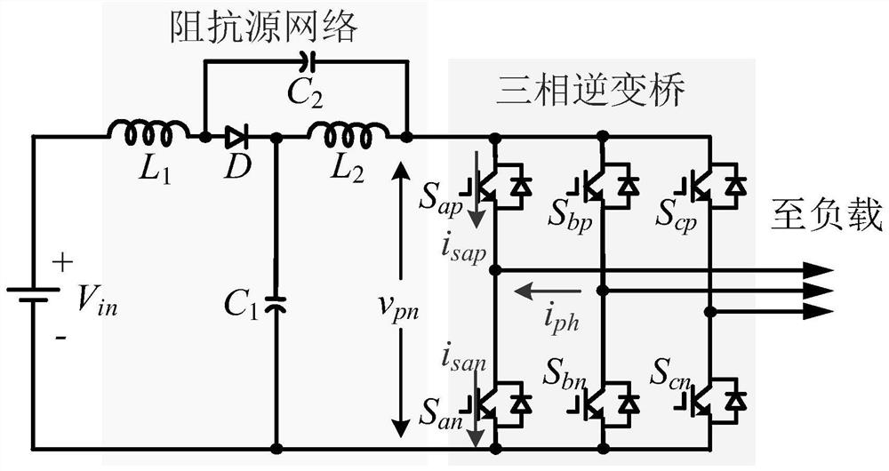
A switching device and current stress technology, applied in the direction of converting AC power input to DC power output, electrical components, output power conversion devices, etc., can solve the complex gate-level signal generation process, large current stress of switching devices, switching devices The number of times of flow is too high to achieve the effect of prolonging life, reducing the number of times of flow change, and simplifying the generation process

Active Publication Date: 2021-03-16
珠海创芯科技有限公司
View PDF4 Cites 1 Cited by
  • Summary
  • Abstract
  • Description
  • Claims
  • Application Information

AI Technical Summary

Problems solved by technology

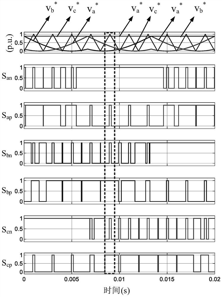
[0011] (1) The number of commutation times of the switching device is large, which leads to an increase in the switching loss of the device;
[0012] (2) The traditional SVPWM modulation strategy needs to use 5 reference signals, which makes the generation process of the gate-level signal that controls the device to be turned on or off more complicated;
[0013] (3) The continuous commutation of switching devices in the fundamental frequency period will lead to a large current stress on the switching devices of some quasi-Z source inverters using traditional modulation strategies

Method used


Image

  • Modulation method for improving current stress of quasi-Z-source inverter switching device
  • Modulation method for improving current stress of quasi-Z-source inverter switching device
  • Modulation method for improving current stress of quasi-Z-source inverter switching device

Examples


Embodiment Construction

[0044] The present invention will be clearly and completely described below in conjunction with the accompanying drawings and embodiments, and the technical problems and beneficial effects solved by the technical solutions of the present invention are also described. It should be pointed out that the described embodiments are only intended to facilitate the implementation of the present invention understood without any limitation.

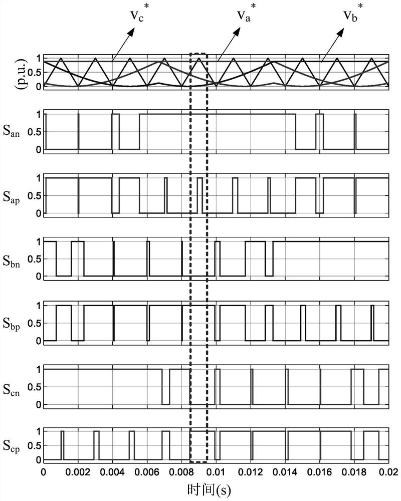
[0045] The modulation method for improving the current stress of the switching device of the quasi-Z source inverter of the present invention is based on the improved simple step-up space vector modulation (SBMSV) modulation strategy, and the single-phase bridge arm straight-through is changed into the three-phase bridge arm straight-through, thereby Realize the function of reducing the current stress of the switching device. The specific modulation method of this method is as follows:

[0046] The modulation wave of the modulation method of the p...


PUM


Abstract

The invention provides a modulation method for improving the current stress of a quasi-Z-source inverter switching device, and the modulation method comprises the steps: subtracting the maximum valueof saddle waves from saddle waves of a conventional voltage space vector modulation SVPWM with the phase difference of 120 degrees to obtain three modulating waves, wherein the maximum value of three-phase saddle waves is a straight line according to the converted waveform, and translating the straight line upwards for M / 2, wherein M is the distance between the maximum value and the minimum valueof the modulated wave after the modulated wave and the triangular carrier wave are subjected to per-unit processing between 0 and 1. According to the modulation method, the gate-level signal generation process is simple, the switching loss is low, no low-frequency alternating-current component exists on the input direct-current side, the current stress of the switching device is greatly reduced, and the service life of the switching device is prolonged.

Description

technical field [0001] The invention belongs to the field of inverter control, and more specifically relates to a modulation method for improving the current stress of a switch device of a quasi-Z source inverter. Background technique [0002] With the increasingly prominent environmental problems, countries are vigorously developing new energy industries. The mainstream inverter topology in the field of new energy is the voltage source inverter (Voltage source inverter, VSI), which is evolved from a buck converter and can only work in buck mode. In order to meet the wide-range voltage input of the rear inverter, the new energy power generation system usually adopts the structure of DC-DC conversion circuit + inverter. This kind of multi-level converter has large energy loss, and has limitations in terms of conversion efficiency, reliability and cost. On the other hand, the upper and lower switching tubes of the same VSI bridge arm cannot be turned on at the same time, oth...

Claims


Application Information

Patent Timeline
IPC IPC(8): H02M7/5387H02M7/5395
CPCH02M7/53875H02M7/5395
Inventor 谭天诚刘平张桂斌谭天利吴刚吴文昊
Owner 珠海创芯科技有限公司
Learn More