Electrostatic protection circuit and display panel

An electrostatic protection and circuit technology, applied in circuits, electrical components, electrical solid devices, etc., can solve the problems of difficulty in charge release and small layout area, and achieve the effect of large leakage current and improved reliability.

Active Publication Date: 2021-03-19
TCL CHINA STAR OPTOELECTRONICS TECH CO LTD
View PDF5 Cites 0 Cited by
  • Summary
  • Abstract
  • Description
  • Claims
  • Application Information

AI Technical Summary

Problems solved by technology

Oxide TFT-based GOA (Gate Driver on Array, array substrate row drive) circuit Oxide TFT has high mobility, TFT can achieve a smaller layout area (layout area), which is helpful for making narrow border panels, However, the low oxide leakage current also makes it difficult to release the charge in the GOA signal line. Compared with a-Si products, the GOA circuit signal line of the oxide TFT panel has ESD (Electro-Static Discharge, electrostatic discharge) higher risk

Method used


Image

  • Electrostatic protection circuit and display panel
  • Electrostatic protection circuit and display panel
  • Electrostatic protection circuit and display panel

Examples


Embodiment Construction

[0028] In order to make the technical solutions and advantages of the present invention clearer, the implementation manners of the present invention will be further described in detail below in conjunction with the accompanying drawings. Apparently, the described embodiments are only a part of the embodiments of the present application, and are not exhaustive of all the embodiments. It should be noted that, in the case of no conflict, the embodiments in the present application and the features in the embodiments can be combined with each other.

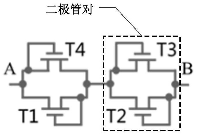
[0029] After analyzing and researching the existing technologies, such as figure 1 As shown, without changing the specific structure of the TFT, the TFT in the electrostatic protection circuit can be connected in the form of a diode pair (diode pair), which is equivalent to increasing the channel width-to-length ratio of the TFT, so as to achieve the adjustment of the electrostatic protection circuit. purpose of leakage current magni...


PUM


Abstract

The invention discloses an electrostatic protection circuit and a display panel. The electrostatic protection circuit comprises: a first voltage reference unit which is used for carrying out the primary voltage division of a voltage between a row drive signal line and a common electrode line of an array substrate; a second voltage reference unit which is used for carrying out secondary voltage division on the voltage between the array substrate row driving signal line and the common electrode line; and a charge release unit which is used for adjusting charge distribution between the array substrate row driving signal line and the common electrode line based on the reference voltage provided by the first voltage reference unit and the second voltage reference unit. Compared with existing electrostatic protection circuits, the electrostatic protection circuit has larger leakage current under the condition of high voltage, can release accumulated electrostatic charges of row driving signal lines of the array substrate in time, and avoids the phenomenon of cross-line electrostatic breakdown of the circuit. When the circuit works normally at low voltage, the load of the array substraterow driving signal lines is not affected, and the reliability of the display panel is improved.

Description

technical field [0001] The invention relates to the field of display technology. More specifically, it relates to an electrostatic discharge protection circuit and a display panel. Background technique [0002] Oxide semiconductors represented by IGZO (indium gallium zinc oxide) are channel layer materials used in the new generation of TFT (Thin Film Transistor, Thin Film Field Effect Transistor) technology. Oxide TFTs have relatively high mobility High, good uniformity, low manufacturing cost and other advantages and in large-size AMLCD (Active Matrix Liquid Crystal Display, active matrix color liquid crystal display), AMOLED (Active-matrix organic light emitting diode, active matrix organic light emitting diode) and other displays It has wide application prospect in the panel. Compared with a-Si TFT (Amorphous Silicon Thin Film Field Effect Transistor), oxide TFT not only has higher mobility, but also has lower leakage current I off Therefore, the display pixels using o...

Claims


Application Information

Patent Timeline
Patent Type & Authority Applications(China)
IPC IPC(8): H01L27/02H01L27/12H01L27/32G02F1/1362G02F1/1368
CPCH01L27/0248H01L27/1214H01L27/1225G02F1/136204G02F1/1368H10K59/12G09G2300/0408G09G2330/04G09G2320/0219G09G3/2096G09G2300/08G09G2300/0426H02H7/20H02H9/04
Inventor 李育智
Owner TCL CHINA STAR OPTOELECTRONICS TECH CO LTD
Why Eureka
Try Eureka