

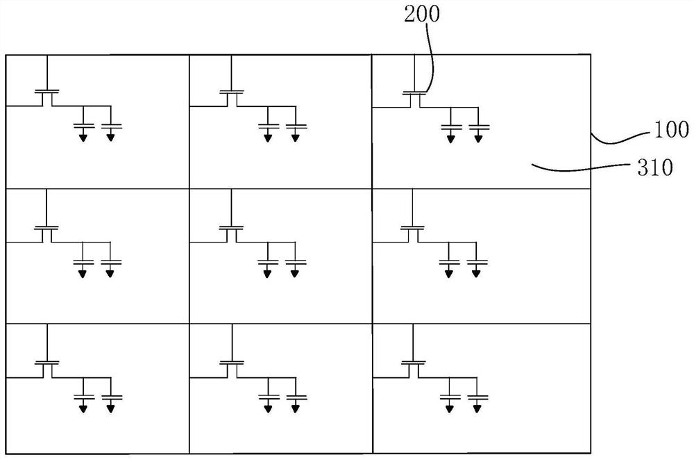
Active switch, manufacturing method thereof and display panel
A production method and active technology, applied in semiconductor/solid-state device manufacturing, optics, instruments, etc., can solve problems such as poor performance of thin film transistors and unstable characteristics of active layers, so as to prevent leakage current, improve leakage effect, and improve The effect of stability
- Summary
- Abstract
- Description
- Claims
- Application Information
AI Technical Summary
Problems solved by technology
Method used
Image

Examples
Embodiment Construction
[0034] It should be understood that the terminology and specific structural and functional details disclosed herein are representative only for describing specific embodiments, but the application can be embodied in many alternative forms and should not be construed as merely Be limited by the examples set forth herein.
[0035] In the description of the present application, the terms "first" and "second" are used for descriptive purposes only, and cannot be understood as indicating relative importance, or implicitly indicating the quantity of indicated technical features. Therefore, unless otherwise specified, the features defined as "first" and "second" may explicitly or implicitly include one or more of these features; "plurality" means two or more. The term "comprising" and any variations thereof mean non-exclusive inclusion, possible presence or addition of one or more other features, integers, steps, operations, units, components and / or combinations thereof.
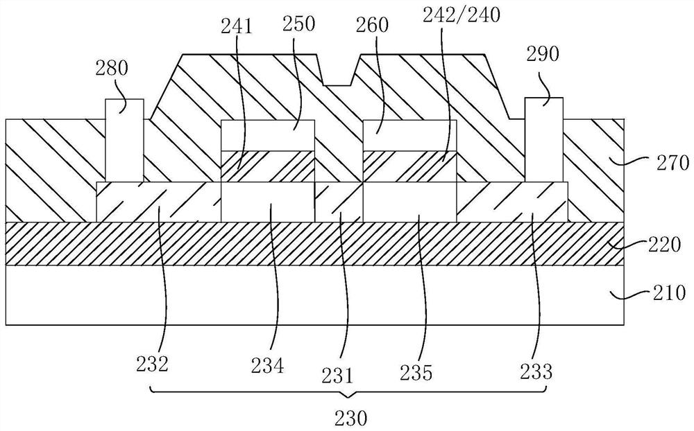
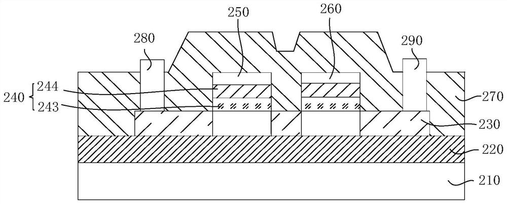
[0036] Al...
PUM
 Abstract
Description
Claims
Application Information