
Multilayer circuit board, board body and processing method of board body

A technology of multi-layer circuit board and processing method, which is applied in multi-layer circuit manufacturing, processing of insulating substrate/layer, printed circuit, etc., can solve the problems affecting the flatness of circuit board, cumbersome production process, and long process flow, etc. Achieve the effect of improving conductivity and stability, simplifying production procedures, and simple production process

Pending Publication Date: 2021-03-23
HUIZHOU TECHUANG ELECTRONIC TECH CO LTD
View PDF13 Cites 2 Cited by
  • Summary
  • Abstract
  • Description
  • Claims
  • Application Information

AI Technical Summary

Problems solved by technology

[0003] However, the existing high-density interconnected printed circuit boards require multiple processes to process the circuit boards to form the required shapes of blind holes, slots and other surface treatments.
For conventional multi-layer stacked circuit boards, the production process is relatively long, and multiple pressings are required in the production process. After each pressing, drilling, hole filling and electroplating are performed multiple times, so as to achieve multi-level lead-through. Generally, especially in the production of high-density interconnected printed circuit boards above the second order, the production process is cumbersome and the process flow is long. Poor connection is prone to occur, which affects the flatness of the circuit board, and the cumulative alignment deviation will lead to non-conduction and incompatibility of blind holes

Method used


Image

  • Multilayer circuit board, board body and processing method of board body
  • Multilayer circuit board, board body and processing method of board body
  • Multilayer circuit board, board body and processing method of board body

Examples


Embodiment 1

[0107]Select a silver-free PP board with high flatness for the cutting operation, and open two first positioning holes and two second positioning holes on the diagonal positions of the silver-free PP board, each first positioning hole is connected with a The central axis line of the second positioning hole is parallel to the longest side of the silver-free PP board, the distance between the first positioning hole and the longest side of the silver-free PP board is 4.9mm, and the distance between the second positioning hole and the longest side of the silver-free PP board The distance is 4.9mm, and the diameter of the positioning holes is 2mm. After determining the positioning hole, set the pattern of the circuit board on the marking software operation interface to determine the path of laser ablation, and set the laser focus of the laser beam emitted by the laser on the surface of the silver-free PP board to focus the laser energy on one point , where the output power of the l...

Embodiment 2

[0109] Select a silver-free PP board with high flatness for the cutting operation, and open two first positioning holes and two second positioning holes on the diagonal positions of the silver-free PP board, each first positioning hole is connected with a The central axis line of the second positioning hole is parallel to the longest side of the silver-free PP board, the distance between the first positioning hole and the longest side of the silver-free PP board is 5.0mm, and the distance between the second positioning hole and the longest side of the silver-free PP board The distance is 5.0mm, and the diameter of the positioning holes is 2.5mm. After determining the positioning hole, set the pattern of the circuit board on the marking software operation interface to determine the path of laser ablation, and set the laser focus of the laser beam emitted by the laser on the surface of the silver-free PP board to focus the laser energy on one point , where the output power of th...

Embodiment 3

[0111] Select a silver-free PP board with high flatness for the cutting operation, and open two first positioning holes and two second positioning holes on the diagonal positions of the silver-free PP board, each first positioning hole is connected with a The central axis line of the second positioning hole is parallel to the longest side of the silver-free PP board, the distance between the first positioning hole and the longest side of the silver-free PP board is 5.1mm, and the distance between the second positioning hole and the longest side of the silver-free PP board The distance is 5.1mm, and the diameter of the positioning holes is 3mm. After determining the positioning hole, set the pattern of the circuit board on the marking software operation interface to determine the path of laser ablation, and set the laser focus of the laser beam emitted by the laser on the surface of the silver-free PP board to focus the laser energy on one point , where the output power of the ...


PUM


Abstract

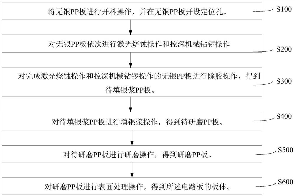
The invention provides a multilayer circuit board, a board body and a processing method of the board body. The processing method of the board body of the circuit board comprises the following steps of: carrying out cutting operation on a silver-free PP board, and forming a positioning hole in the silver-free PP board; sequentially carrying out laser ablation operation and depth-control mechanicaldrilling and milling operation on the silver-free PP board; conducting glue removing operation on the silver-free PP board obtained after completing laser ablation operation and depth-control mechanical drilling and milling operation, so as to obtain a PP board to be filled with silver paste; performing silver paste filling operation on the PP board to be filled with the silver paste to obtain a PP board to be ground; grinding the PP ground to be ground to obtain a ground PP ground; and performing surface treatment operation on the ground PP board to obtain a board body of the circuit board. The method for processing the board body of the circuit board has the advantages of simple process and capabilities of improving the flatness of the circuit board and reducing the thickness of the circuit board.

Description

technical field [0001] The invention relates to the technical field of printed circuit board production, in particular to a multilayer circuit board, a board body and a processing method thereof. Background technique [0002] With the rapid development of electronic products, people's high requirements for product quality have also led to higher and higher requirements for electronic manufacturers on printed circuit boards, and the difficulty of forming and processing boards is becoming more and more difficult. There are more and more requirements for molding, small spacing between sheets, and molding without process edges. Some special motherboards or plug boards even need to be spliced, which requires very high flatness and thickness of the circuit board, and the thickness is suitable for easy plugging or loading. [0003] However, the existing high-density interconnected printed circuit boards require multiple processes to process the circuit boards to form required blin...

Claims


Application Information

Patent Timeline
Patent Type & Authority Applications(China)
IPC IPC(8): H05K3/00H05K3/46
CPCH05K3/0044H05K3/0052H05K3/46
Inventor 许校彬
Owner HUIZHOU TECHUANG ELECTRONIC TECH CO LTD
Learn More