Composite substrate and preparation method thereof and electronic component

A technology of electronic components and composite substrates, applied in the direction of electrical components, impedance networks, etc., can solve problems such as radio frequency loss

Active Publication Date: 2021-03-26
JINAN JINGZHENG ELECTRONICS
View PDF13 Cites 0 Cited by
  • Summary
  • Abstract
  • Description
  • Claims
  • Application Information

AI Technical Summary

Problems solved by technology

[0004] This application provides a composite substrate and its preparation method, and electronic components to solve the problem of easy formation of a conductive film layer at the interface between an insulating layer and a semiconductor in the prior art. , and the conductive film layer will interact with the penetrating electromagnetic field due to its proximity to the active layer, resulting in the problem of radio frequency loss

Method used


Image

  • Composite substrate and preparation method thereof and electronic component
  • Composite substrate and preparation method thereof and electronic component
  • Composite substrate and preparation method thereof and electronic component

Examples


preparation example Construction

[0058] Specifically, refer to Figure 5 , the preparation method comprises:

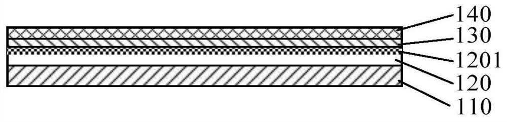
[0059] S11 , prepare the substrate layer 110 .

[0060] This step also includes performing semiconductor-grade RCA cleaning on the substrate layer 110 to obtain a clean surface.

[0061] S12, preparing a microcrystalline layer 100 on the substrate layer.

[0062] Optionally, this step can be obtained by the following methods:

[0063] Under silicon-containing gas or a mixture of silicon-containing gas and other gases, or under germanium-containing gas or a mixture of germanium-containing gas and other gases, microcrystalline grains containing random crystal orientations are grown on the substrate layer 110 The microcrystalline layer 100.

[0064] That is to say, in this step, the substrate in step S11 can be placed in a deposition furnace, and a silicon-containing gas or a mixture of silicon-containing gas and other gases, such as SiH 4 The gas is used to control the growth process conditions to...

Embodiment 1

[0087] 1) Provide a single crystal silicon substrate layer.

[0088] 2) Perform semiconductor-grade RCA cleaning on the single crystal silicon substrate layer to obtain a clean surface.

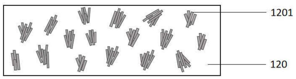
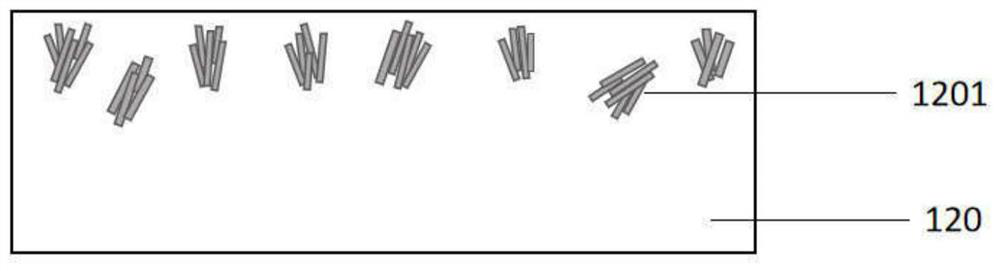
[0089] 3) Place the monocrystalline silicon substrate layer in step 2) in the deposition furnace, and pass through the SiH-containing 4 The gas is used to control the growth process conditions to grow a microcrystalline silicon layer containing microcrystalline grains arranged in random crystal directions, and the distance between microcrystalline grains in the microcrystalline silicon layer is controlled at about 300nm.

[0090] 4) Annealing the microcrystalline silicon layer in step 3) at 800° C. for 5 hours to form a polycrystalline silicon layer with crystal grain clusters with a size of 100 nm to 500 nm.

[0091] 5) An insulating layer is formed on the polysilicon layer obtained in step 4).

[0092] 6) Polishing the insulating layer in step 5) to obtain a smooth surface.

[0093] 7) P...

Embodiment 2

[0095] 1) Provide a single crystal silicon substrate layer.

[0096] 2) Perform semiconductor-grade RCA cleaning on the single crystal silicon substrate layer to obtain a clean surface.

[0097] 3) Place the monocrystalline silicon substrate layer in step 2) in the deposition furnace, and pass through the SiH-containing 4 The gas is used to control the growth process conditions to grow a microcrystalline silicon layer containing microcrystalline grains arranged in random crystal directions, and the distance between microcrystalline grains in the microcrystalline silicon layer is controlled at about 1000nm.

[0098] 4) Annealing the microcrystalline silicon layer in step 3) at 950° C. for 10 h to form a polycrystalline silicon layer with crystal grain clusters with a size of 500 nm to 1000 nm.

[0099] 5) An insulating layer is formed on the polysilicon layer obtained in step 4).

[0100] 6) Polishing the insulating layer in step 5) to obtain a smooth surface.

[0101] 7) A ...


PUM

PropertyMeasurementUnit
diameteraaaaaaaaaa
grain sizeaaaaaaaaaa
electrical resistivityaaaaaaaaaa

Abstract

The invention provides a composite substrate and a preparation method thereof and an electronic component, and the composite substrate sequentially comprises a substrate layer, a polycrystalline layer, an insulating layer and a thin film layer from the bottom to the top. The polycrystalline layer is provided with a crystal grain cluster composed of two or more crystal grains. According to the scheme, the polycrystalline layer with the grain cluster structure is arranged between the insulating layer and the substrate layer, a large number of defects formed in the grain cluster can capture charged carriers, the carriers are gathered at the grain boundary to form a potential barrier between grains, movement of the carriers between the grains is limited, and therefore, the interface conductionbetween the insulating layer and the semiconductor layer can be reduced, and the radio frequency loss is reduced.

Description

technical field [0001] The present application relates to the field of semiconductor technology, in particular to a composite substrate, a preparation method thereof, and electronic components. Background technique [0002] Composite piezoelectric substrates used in RF surface acoustic wave filters generally include a piezoelectric layer, a low-sonic layer, a high-sonic layer and a substrate layer. Among them, the setting of the high and low sound velocity layers can greatly suppress the leakage of sound wave energy into the substrate and reduce the loss of the device. The piezoelectric layer is a functional layer, also known as the active layer, which is used to realize the mutual conversion of electricity and sound; the high sound velocity difference generated by the low sound velocity layer and the high sound velocity layer can suppress the leakage of sound waves to the substrate and reduce the overall device loss , and the single crystal silicon substrate has high sound...

Claims


Application Information

Patent Timeline
Patent Type & Authority Applications(China)
IPC IPC(8): H03H3/10H03H9/02H03H9/25H03H9/64
CPCH03H3/10H03H9/02559H03H9/02566H03H9/02574H03H9/02622H03H9/25H03H9/64
Inventor 李真宇杨超张秀全李洋洋韩智勇
Owner JINAN JINGZHENG ELECTRONICS
Why Eureka
Try Eureka