Preparation method of erasable bulk phase grating
A technology of grating and processing method, which is applied in the field of grating to achieve the effects of flat and smooth surface, multi-grating diffraction function and strong scratch resistance.
- Summary
- Abstract
- Description
- Claims
- Application Information
AI Technical Summary
Problems solved by technology
Method used
Image
Examples
Embodiment 1
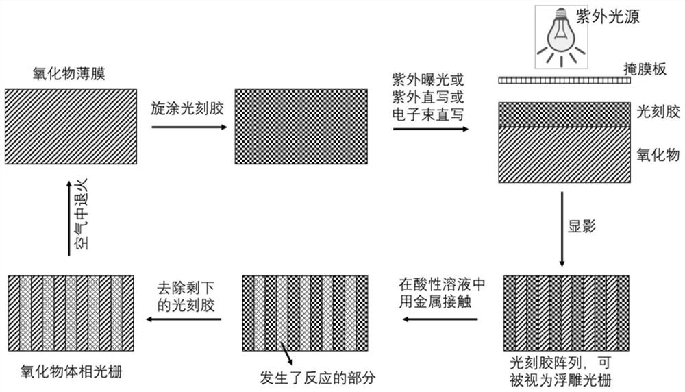
[0045] Step 1. Spin-coat a 2.5 μm thick S1813 positive photoresist layer on a tungsten oxide film with a thickness of 260 nm and a size of 1 cm×1 cm, and then bake it on a heating plate at 115° C. for one minute.
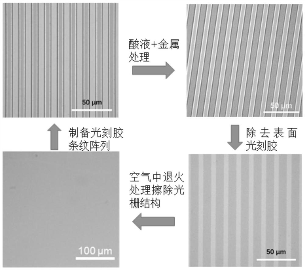
[0046] Step 2. Let the intensity be 19.5mW / cm 2 The ultraviolet light is exposed to the photoresist layer through a mask plate with a stripe pattern, the exposure time is 7.5s, and the interval period of the stripes on the mask plate is 8 μm. Then immerse the exposed tungsten oxide film covered with photoresist layer in a developing solution for development, thereby forming a striped photoresist array on the surface of the tungsten oxide film, such as figure 2 .
[0047] Step 3, immerse the tungsten oxide film covered with the striped photoresist array in the dilute sulfuric acid solution with a concentration of 2% wt, and then allow the zinc wire to contact the surface of the film to react for at least 5 minutes. The surface of the tungsten oxide film not covere...
Embodiment 2
[0052] Step 1. Spin-coat a 2.5 μm thick NR9-3000PY negative photoresist layer on a tungsten oxide film with a thickness of 260nm and a size of 1cm×1cm, and then bake it on a heating plate at 120°C for one minute.
[0053] Step 2. Let the intensity be 19.5mW / cm 2 The ultraviolet light is exposed to the photoresist layer through a mask plate with a square pattern, the exposure time is 20s, and the horizontal and vertical intervals of the block shape on the mask plate are both 8 μm. Then, the tungsten oxide film covered with photoresist layer after exposure is immersed in a developing solution for development, thereby forming a square photoresist periodic array on the surface of the tungsten oxide film ( Figure 6 shown). Submerge the tungsten oxide film covered with square photoresist arrays in dilute sulfuric acid solution with a concentration of 2% wt, and then let the zinc wire touch the surface of the film to react for more than 5 minutes. The surface of the tungsten oxide...
PUM
 Abstract
Description
Claims
Application Information
 - R&D Engineer
- R&D Manager
- IP Professional
- Industry Leading Data Capabilities
- Powerful AI technology
- Patent DNA Extraction
Browse by: Latest US Patents, China's latest patents, Technical Efficacy Thesaurus, Application Domain, Technology Topic, Popular Technical Reports.
© 2024 PatSnap. All rights reserved.Legal|Privacy policy|Modern Slavery Act Transparency Statement|Sitemap|About US| Contact US: help@patsnap.com


