
N-type monocrystalline silicon HBC solar cell structure and preparation method thereof

A technology for solar cells and monocrystalline silicon, applied in circuits, electrical components, photovoltaic power generation, etc., can solve problems such as high production costs and difficult manufacturing processes, reduce minority carrier recombination, improve passivation effects and anti-reflection effects, and increase The effect of n+ front field area

Inactive Publication Date: 2021-04-09
ZHEJIANG AIKO SOLAR ENERGY TECH CO LTD +2
View PDF3 Cites 0 Cited by
  • Summary
  • Abstract
  • Description
  • Claims
  • Application Information

AI Technical Summary

Problems solved by technology

[0003] Solar cells are the core part of solar power generation. The existing HBC cell structure adopts a-Si+SiNx film layer structure on the front, lacks doping layer for field passivation; the fabrication of the interdigitated p-n junction structure on the back requires repeated fabrication of masks Then remove the mask, and need to deposit amorphous silicon film multiple times, the manufacturing process is difficult and the production cost is high

Method used


Image

  • N-type monocrystalline silicon HBC solar cell structure and preparation method thereof
  • N-type monocrystalline silicon HBC solar cell structure and preparation method thereof
  • N-type monocrystalline silicon HBC solar cell structure and preparation method thereof

Examples


Embodiment 1

[0055] The preparation method of the above-mentioned N-type monocrystalline silicon HBC solar cell structure of the present invention comprises the following steps:

[0056] Step (1): Select an N-type single crystal silicon wafer, use the existing conventional method to carry out texturing on the front and polishing on the back to obtain a silicon wafer with a front reflectivity of 9%-15% and back polishing, and the obtained silicon wafer is The single crystal silicon substrate 4 of the battery; the polishing technology adopts chemical liquid polishing, and physical polishing can also be used;

[0057] Step (2): Place the silicon wafer obtained in step (1) in a furnace tube at 950°C for boron diffusion. The silicon wafers are placed face to face, and the diffusion time is 65 minutes. The diffusion time can also be selected within the range of 60-70 minutes , diffused on the back of the silicon wafer to form a p+-type crystalline silicon layer 5, with a diffusion square resista...

Embodiment 2

[0074] The preparation method of the above-mentioned N-type monocrystalline silicon HBC solar cell structure of the present invention comprises the following steps:

[0075] Step (1): Select an N-type single crystal silicon wafer, use the existing conventional method to carry out texturing on the front and polishing on the back to obtain a silicon wafer with a front reflectivity of 9%-15% and back polishing, and the obtained silicon wafer is The monocrystalline silicon substrate 4 of the battery;

[0076] Step (2): place the silicon wafer obtained in step (1) in a furnace tube at 950°C for boron diffusion, place the silicon wafers face to face, and diffuse for 70 minutes to form a p+ type crystalline silicon layer 5 on the back of the silicon wafer. Diffusion square resistance 150Ω±10Ω;

[0077] Step (3): Place the silicon wafer obtained in step (2) in a furnace tube at 850°C for boron diffusion. The silicon wafers are placed back to back, and the diffusion time is 70 minutes...

Embodiment 3

[0092] The preparation method of the above-mentioned N-type monocrystalline silicon HBC solar cell structure of the present invention comprises the following steps:

[0093] Step (1): Select an N-type single crystal silicon wafer, use the existing conventional method to carry out texturing on the front and polishing on the back to obtain a silicon wafer with a front reflectivity of 9%-15% and back polishing, and the obtained silicon wafer is The single crystal silicon substrate 4 of the battery; the polishing technology adopts chemical liquid polishing, and physical polishing can also be used;

[0094] Step (2): Place the silicon wafer obtained in step (1) in a furnace tube at 950°C for boron diffusion. The silicon wafers are placed face to face, and the diffusion time is 65 minutes. The diffusion time can also be selected within the range of 60-70 minutes , diffused on the back of the silicon wafer to form a p+-type crystalline silicon layer 5, with a diffusion square resista...


PUM


Abstract

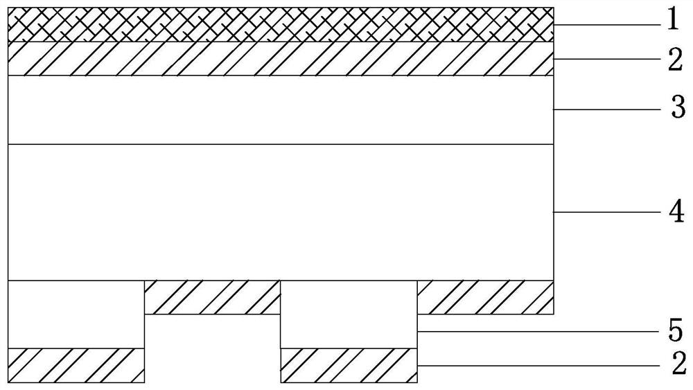
The invention discloses an N-type monocrystalline silicon HBC solar cell structure and a preparation method thereof. The cell structure comprises a monocrystalline silicon substrate, a front surface structure and a back surface structure, the front surface structure comprises a silicon nitride layer, a silicon oxide layer and an n+ type crystalline silicon layer which are arranged from top to bottom, and the back surface structure comprises two unit structures which are alternately arranged left and right. Each unit structure comprises a p+ type crystalline silicon layer, a TCO conducting film and a metal electrode which are arranged from top to bottom, the other unit structure comprises an intrinsic amorphous silicon layer, an n+ amorphous silicon layer, a TCO conducting film and a metal electrode which are arranged from top to bottom, and the thickness of the p+ type crystalline silicon layer is equal to the sum of the thickness of the intrinsic amorphous silicon layer and the thickness of the n+ amorphous silicon layer. The TCO conducting films of the two unit structures are equal in thickness and are arranged in parallel, and a gap is reserved between the TCO conducting films. The cell structure can improve the passivation effect and the antireflection effect of the front surface. The invention also discloses the preparation method of the battery structure.

Description

technical field [0001] The invention relates to a silicon wafer and a preparation method thereof, in particular to an N-type monocrystalline silicon HBC solar cell structure and a preparation method thereof. Background technique [0002] Energy is the cornerstone of the development of modern society. With the continuous development of the global economy and society, energy consumption continues to grow. Over time, fossil energy is becoming more and more scarce. In the context of fossil energy shortages, large-scale development and Inventing renewable resources has become an important strategy for future energy, and solar energy is the cleanest clean energy, renewable energy. [0003] Solar cells are the core part of solar power generation. The existing HBC cell structure adopts a-Si+SiNx film layer structure on the front, lacks doping layer for field passivation; the fabrication of the interdigitated p-n junction structure on the back requires repeated fabrication of masks ...

Claims


Application Information

Patent Timeline
Patent Type & Authority Applications(China)
IPC IPC(8): H01L31/072H01L31/0352H01L31/0376H01L31/20
CPCH01L31/035272H01L31/03762H01L31/072H01L31/202Y02E10/548Y02P70/50
Inventor 解观超田得雨张小明盛健林纲正陈刚
Owner ZHEJIANG AIKO SOLAR ENERGY TECH CO LTD
Learn More