Passivation structure applied to contact passivation battery and preparation method of passivation structure
A battery and contact technology, applied in the field of solar cells, can solve problems such as large failure rate
- Summary
- Abstract
- Description
- Claims
- Application Information
AI Technical Summary
Problems solved by technology
Method used
Image

Examples
preparation example Construction
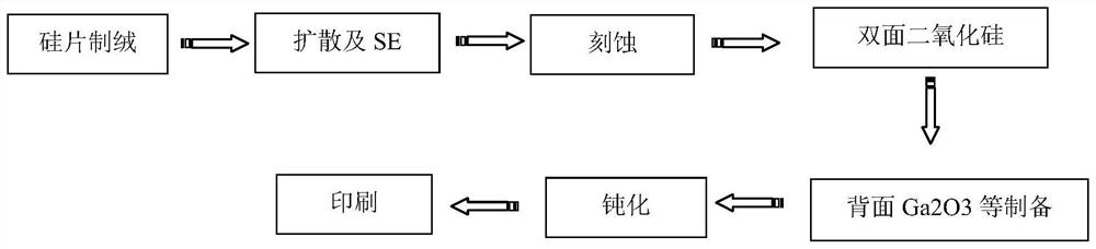
[0040] A method for preparing a passivation structure applied to a contact passivation battery, comprising the following preparation steps:
[0041] A. N-type monocrystalline silicon wafers are used, and groove-type double-sided texturing is adopted, and the weight loss is 0.3-0.35g;
[0042] B. Carry out boron expansion on the front surface, and control the surface concentration to 1E+19-2E+19 / cm 3 ;
[0043] C, using acid (acid is HF or HNO 3 ) removing the back BSG and performing back etching, then cleaning and retaining the front BSG layer, the back etching weight loss is 0.2-0.5g, and the reflectivity after back etching is >32%;
[0044] D. Using tubular oxidation, deposit a layer of SiO with a thickness of 1.4-1.6nm on the back of the silicon wafer 2 layer, and then deposited SiO under gas flow x N y layer, and do in-situ doping at the same time, the rear resistance of doping is about 20-40Ω / sq; the air flow rate is NH 3 with SiH 4 flow ratio or N 2 O and SiH 4 ...
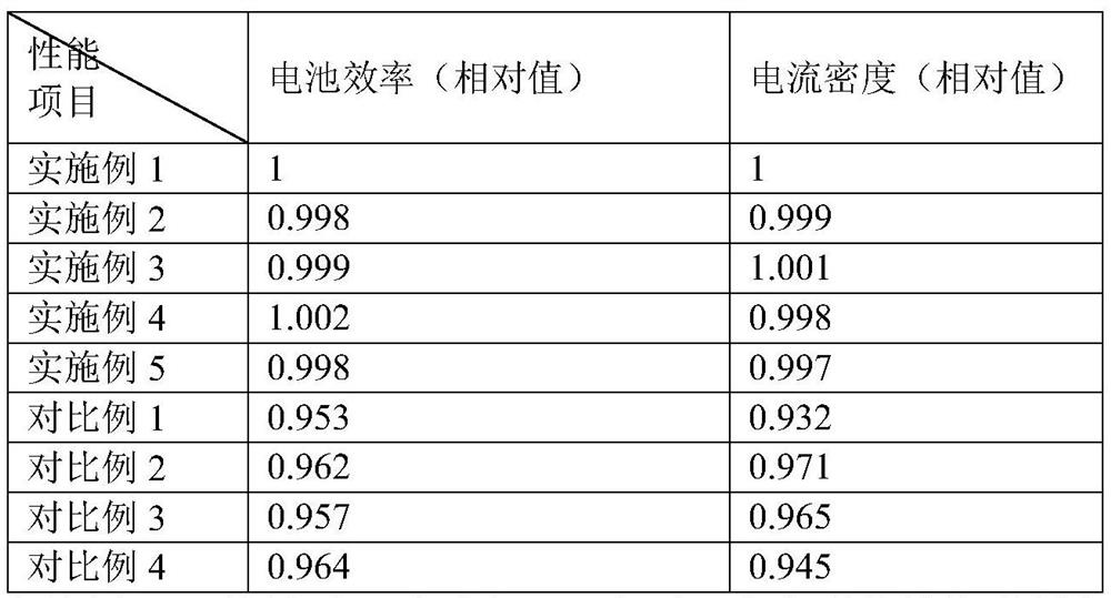
Embodiment 1
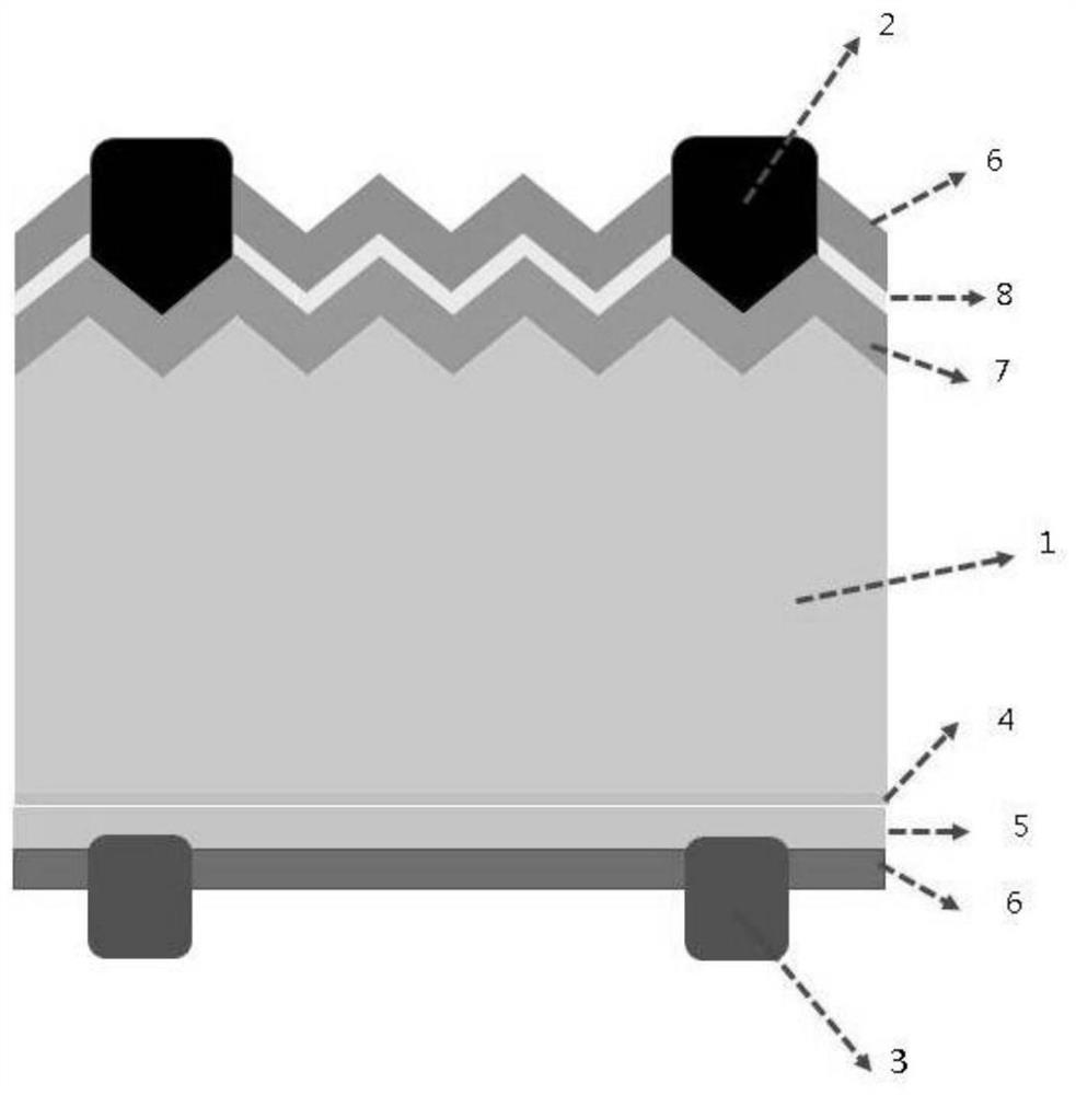
[0049] A passivation structure applied to a contact passivation battery, comprising an N-type substrate 1, two positive electrodes 2 arranged on the front of the N-type substrate 1 and two positive electrodes 2 arranged on the back of the N-type substrate 1 Negative electrode 3, the back side of the N-type substrate 1 is provided with SiO 2 Layer 4, the SiO 2 Layer 4 is provided with doped polycrystalline SiO x N y Layer 5.
[0050] The front side of the N-type substrate 1 is sequentially provided with a P+ layer 7, AlO x Layer 8 and SiN x Layer 6. The positive electrode 2 sequentially passes through the SiN x Layer 6, AlO x Layer 8, in contact with P+ layer 7. The back of the N-type substrate 1 is sequentially provided with SiO 2 Layer 4, doped polycrystalline SiO x N y Layer 5 and SiN x Layer 6. The negative electrode 3 sequentially passes through the SiN x Layer 6 with partial thickness of doped polycrystalline SiO x N y Layer 5, with doped polycrystalline S...
Embodiment 2
[0060] A passivation structure applied to a contact passivation battery, comprising an N-type substrate 1, two positive electrodes 2 arranged on the front of the N-type substrate 1 and two positive electrodes 2 arranged on the back of the N-type substrate 1 Negative electrode 3, the back side of the N-type substrate 1 is provided with SiO 2 Layer 4, the SiO 2 Layer 4 is provided with doped polycrystalline SiO x N y Layer 5.
[0061] The front side of the N-type substrate 1 is sequentially provided with a P+ layer 7, AlO x Layer 8 and SiN x Layer 6. The positive electrode 2 sequentially passes through the SiN x Layer 6, AlO x Layer 8, in contact with P+ layer 7. The back of the N-type substrate 1 is sequentially provided with SiO 2 Layer 4, doped polycrystalline SiO x N y Layer 5 and SiN x Layer 6. The negative electrode 3 sequentially passes through the SiN x Layer 6 with partial thickness of doped polycrystalline SiO x N y Layer 5, with doped polycrystalline S...
PUM
| Property | Measurement | Unit |
|---|---|---|
| Thickness | aaaaa | aaaaa |
Abstract
Description
Claims
Application Information
 - R&D
- Intellectual Property
- Life Sciences
- Materials
- Tech Scout
- Unparalleled Data Quality
- Higher Quality Content
- 60% Fewer Hallucinations
Browse by: Latest US Patents, China's latest patents, Technical Efficacy Thesaurus, Application Domain, Technology Topic, Popular Technical Reports.
© 2025 PatSnap. All rights reserved.Legal|Privacy policy|Modern Slavery Act Transparency Statement|Sitemap|About US| Contact US: help@patsnap.com