Broadband frequency multiplier with transconductance enhancement technology and double-LC matching network

A matching network and transconductance enhancement technology, applied in power oscillators, electrical components, etc., can solve the problems of matching network loss, low signal output power and efficiency, occupied area, etc., to improve output power and efficiency, and ensure bandwidth performance. , the effect of improving broadband performance

Pending Publication Date: 2021-04-16
UNIV OF ELECTRONIC SCI & TECH OF CHINA
View PDF6 Cites 1 Cited by
  • Summary
  • Abstract
  • Description
  • Claims
  • Application Information

AI Technical Summary

Problems solved by technology

[0005] (1) The imaginary part of the input impedance of the frequency multiplier changes quickly and the matching bandwidth is narrow; the input ports of the structure are all MOSFET gates, the transistor size is small, the imaginary part of the input impedance is large, and the change is drastic; microstrip transmission line matching is used, although there are A certain broadband effect, but it takes up a lot of area, and the matching network also brings a lot of loss;
[0006] (2) The broadband frequency multiplier uses the nonlinearity of the transistor to extract the second harmonic signal. Since the second harmonic is smaller than the fundamental signal, the output power and efficiency of the signal are lower;
[0007] (3) It is difficult to achieve broadband matching effect by using a single LC impedance matching network for the output of the broadband frequency multiplier

Method used


Image

  • Broadband frequency multiplier with transconductance enhancement technology and double-LC matching network
  • Broadband frequency multiplier with transconductance enhancement technology and double-LC matching network
  • Broadband frequency multiplier with transconductance enhancement technology and double-LC matching network

Examples


Embodiment Construction

[0026] The present invention will be described in further detail below in conjunction with the accompanying drawings and embodiments.

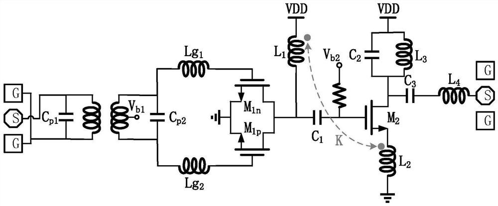
[0027] This embodiment provides a broadband frequency multiplier with transconductance enhancement technology and double LC matching network, its circuit principle is as follows figure 1 As shown, it is mainly composed of four parts: input matching network, double frequency stage, common source buffer, and broadband output matching network; among them,

[0028] The doubler stage consists of transistor M 1n , Transistor M 1p , inductance L 1 Composition, Transistor M 1n with transistor M 1p The source of the transistor is connected to ground, and the transistor M 1n with transistor M 1p connected to the drain and connected to the inductor L 1 , inductance L 1 The other end of the power supply voltage VDD;

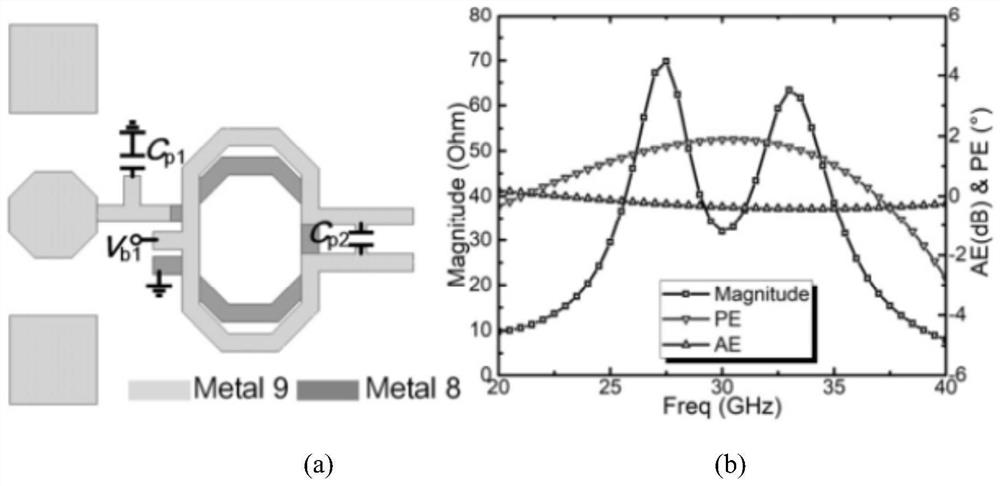
[0029] The input matching network consists of an inductor Lg 1 , inductance Lg 2 , capacitance C p1 , capacitance C p2 And th...


PUM


Abstract

The invention belongs to the technical field of millimeter wave communication, and relates to a frequency multiplier in a frequency source, in particular to a broadband frequency multiplier with a transconductance enhancement technology and a double-LC matching network, which is used for solving the problems of narrow bandwidth, lower output power, lower efficiency and the like of the traditional broadband frequency multiplier. The multiplier is composed of an input matching network, a second harmonic generation stage, a common source buffer and a broadband output matching network. The input matching network adopts a four-order matching network, and inductance of an input impedance imaginary part can be reduced by matching, so that bandwidth performance of the frequency multiplier is guaranteed; meanwhile, the broadband output matching network adopts a double-LC output matching network consisting of a shunt network and a series network, so that the broadband performance of the circuit is improved; in addition, a transconductance enhancement technology is used for coupling a load inductor of a double frequency stage and a source stage inductor of a common source amplifier serving as a buffer stage, so that the output power and efficiency are improved; the broadband performance of the frequency multiplier is improved, and the output power and efficiency of the frequency multiplier are effectively improved.

Description

technical field [0001] The invention belongs to the technical field of millimeter wave communication, relates to a frequency multiplier in a frequency source, and specifically provides a broadband frequency multiplier with a transconductance enhancement technology and a double LC matching network. Background technique [0002] With the development of wireless communication technology, people have higher and higher requirements for the amount of information, so the working frequency is also getting higher and higher. In order to support multi-band services and multi-standard applications, ultra-wide working bandwidth has become the priority of this type of wireless system. Great need. In addition, such 5G systems will require complex modulation schemes, even up to 256-QAM, which place stringent requirements on the linearity, SNR, and LO phase noise of the RF circuit. [0003] In order to meet the development and application of millimeter wave communication, a local oscillato...

Claims


Application Information

Patent Timeline
IPC IPC(8): H03B19/14H03B1/00
Inventor 康凯黄盛吴韵秋赵晨曦刘辉华余益明
Owner UNIV OF ELECTRONIC SCI & TECH OF CHINA
Why Eureka
Try Eureka