Simulation method for wet chemical etching process of flexible PCB

A PCB board and wet chemical technology, which is applied in the field of flexible PCB board preparation and flexible PCB board wet chemical etching process simulation, can solve the problems of relying on manual experiments, high cost, and long time consumption

Active Publication Date: 2021-04-20
WUHAN UNIV
View PDF8 Cites 2 Cited by
  • Summary
  • Abstract
  • Description
  • Claims
  • Application Information

AI Technical Summary

Problems solved by technology

[0005] Aiming at the existing problems in the parameterized analysis of etching process in the existing production process, such as relying on manual experiments, high cost, long time-consuming, blindness, etc., the present invention proposes an etching process simulation method for flexible PCB board production

Method used


Image

  • Simulation method for wet chemical etching process of flexible PCB
  • Simulation method for wet chemical etching process of flexible PCB
  • Simulation method for wet chemical etching process of flexible PCB

Examples


Embodiment Construction

[0036] In order to facilitate the understanding of the embodiments of the present invention, specific embodiments will be taken as examples for further explanation below in conjunction with the accompanying drawings, and each embodiment does not constitute a limitation to the embodiments of the present invention.

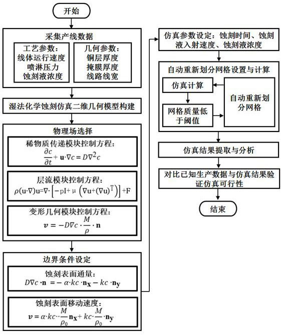
[0037] The copper film is used as the etching substrate below, and the CuCl 2 The solution will be described as an etching solution as an example.

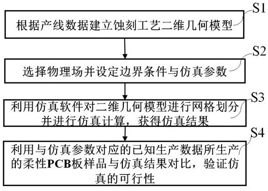
[0038] Such as figure 1 As shown, a method for simulating a flexible PCB wet chemical etching process provided in this embodiment includes the following steps:

[0039] S1, establish a two-dimensional geometric model of the etching process according to the production line data;

[0040] S2, select the physical field module and set boundary conditions and simulation parameters;

[0041] S3, using simulation software to mesh the two-dimensional geometric model and perform simulation calculations to obtain simulation r...


PUM


Abstract

The invention discloses a method for simulating a wet chemical etching process of a flexible PCB (Printed Circuit Board). The method mainly introduces a method for simulating the running speed of a linear body, the spraying pressure and the concentration of etching liquid in the etching process by establishing a model. The specific implementation process is as follows: constructing a two-dimensional geometric model of a copper substrate to be processed by using multi-physical field coupling simulation software COMSOL Multiphysics, setting corresponding simulation parameters and boundary conditions, obtaining a simulation result through simulation calculation, and finally, carrying out experiment verification on the feasibility of simulation by using known production data. According to the method, the material and time cost for researching the wet chemical etching process of the flexible PCB in an experimental mode can be greatly reduced, and the problems existing in the actual production process can be analyzed in a targeted mode.

Description

technical field [0001] The invention belongs to the field of optoelectronics and relates to a flexible PCB board preparation technology, in particular to a flexible PCB board wet chemical etching process simulation method. Background technique [0002] Flexible PCB is a highly reliable and flexible printed circuit board made of polyimide or polyester film, referred to as FPC (Flexible Printed Circuit). Due to its high wiring density, light weight, thin thickness, and good bendability, FPC is widely used in mobile communications, aerospace, military and other fields. The production process of flexible PCB boards generally includes: type punching, coating, exposure, development, etching, film removal, tinning, automatic optical monitoring, ink printing, slitting, circuit testing and final cleaning and packaging. The etching process is a process of removing unnecessary copper on the substrate by wet chemical etching under the protection of a graphic mask to form a circuit diag...

Claims


Application Information

Patent Timeline
Patent Type & Authority Applications(China)
IPC IPC(8): G06F30/398G06F115/12G06F119/14
Inventor 李辉申胜男陈傲杰盛家正
Owner WUHAN UNIV
Why Eureka
Try Eureka