Buck circuit silicon carbide power module

A technology of power modules and silicon carbide, which is applied in the direction of circuits, electrical components, and electric solid-state devices, and can solve problems such as high parasitic inductance, uneven current of switching tubes, and low power density

Pending Publication Date: 2021-04-23
HUAZHONG UNIV OF SCI & TECH
View PDF0 Cites 3 Cited by
  • Summary
  • Abstract
  • Description
  • Claims
  • Application Information

AI Technical Summary

Problems solved by technology

[0005] Aiming at the defects of the prior art, the purpose of the present invention is to provide a buck circuit silicon carbide power module, which aims

Method used


Image

  • Buck circuit silicon carbide power module
  • Buck circuit silicon carbide power module
  • Buck circuit silicon carbide power module

Examples


Embodiment

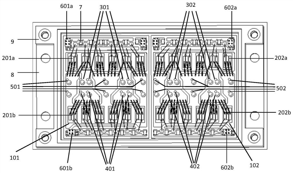
[0024] figure 1 A schematic diagram of the structure of the buck circuit silicon carbide power module provided in this example is shown, the module includes DBC substrates 101 and 102, silicon carbide power chip 201a, silicon carbide power chip 201b, silicon carbide power chip 202a, silicon carbide power chip 202b , positive power terminals 301 and 302, negative power terminals 401 and 402, output power terminals 501 and 502, drive terminal 601a, drive terminal 601b, drive terminal 602a, drive terminal 602b, drive resistor 7, base plate 8 and packaging shell 9. Among them, the silicon carbide power chip 201a and the silicon carbide power chip 201b constitute the first buck half-bridge circuit, which is welded on the DBC substrate 101, and the silicon carbide power chip 202a and the silicon carbide power chip 202b constitute the second buck half-bridge circuit, which is welded on the DBC substrate 102 on.

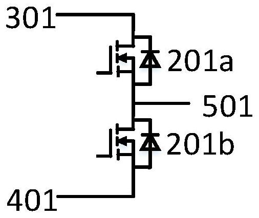
[0025] figure 2 A schematic circuit structure diagram of the first b...


PUM


Abstract

The invention discloses a buck circuit silicon carbide power module, and belongs to the technical field of power electronics. The power module comprises a bottom-layer direct bonded copper DBC substrate, and silicon carbide power chips, a driving resistor, power terminals and driving terminals which are mounted on the bottom-layer DBC substrate. The silicon carbide power chips and the driving resistors form two buck half-bridge circuits. The silicon carbide power chips are connected through metal bonding wires. The bottom-layer DBC substrate is welded on a bottom plate. According to the power module provided by the invention, through reasonable DBC copper layer layout, a current conversion loop is optimized, the balance of a parallel chip loop is realized, the parasitic inductance of the loop is greatly reduced, the size of the module is reduced, and the power density of the module is improved.

Description

technical field [0001] The invention belongs to the technical field of power electronics, and more specifically relates to a buck circuit silicon carbide power module. Background technique [0002] Buck half-bridge circuits are widely used in various electronic devices. However, the power devices used in the existing commercial buck half-bridge modules are still mainly silicon-based devices, the current carrying capacity of the circuit is not high, and the loss is high, so it is not suitable for high-power circuits. [0003] Compared with silicon-based devices, silicon carbide devices have higher current carrying capacity, higher switching speed, lower switching losses, and can operate at higher temperatures. However, the parasitic inductance of the commutation circuit of the existing silicon carbide commercial modules is generally too large, which will increase the switching voltage and current stress on the silicon carbide device. Moreover, the current-carrying capacity ...

Claims


Application Information

Patent Timeline
IPC IPC(8): H01L25/07H01L23/528H01L23/538
CPCH01L25/071H01L23/528H01L23/5386H01L2224/48227H01L2224/0603H01L2224/49111
Inventor 陈材王志伟郭心悦黄志召刘新民康勇
Owner HUAZHONG UNIV OF SCI & TECH
Why Eureka
Try Eureka