

Passivation method of semiconductor device
A semiconductor and device technology, applied in the field of passivation of semiconductor devices, can solve the problems of over-cleaning and incomplete cleaning, and different oxidation degrees of the cavity surface of the bar, so as to achieve uniform thickness and avoid different effects of cleavage time
- Summary
- Abstract
- Description
- Claims
- Application Information
AI Technical Summary
Problems solved by technology
Method used
Image

Examples
Embodiment
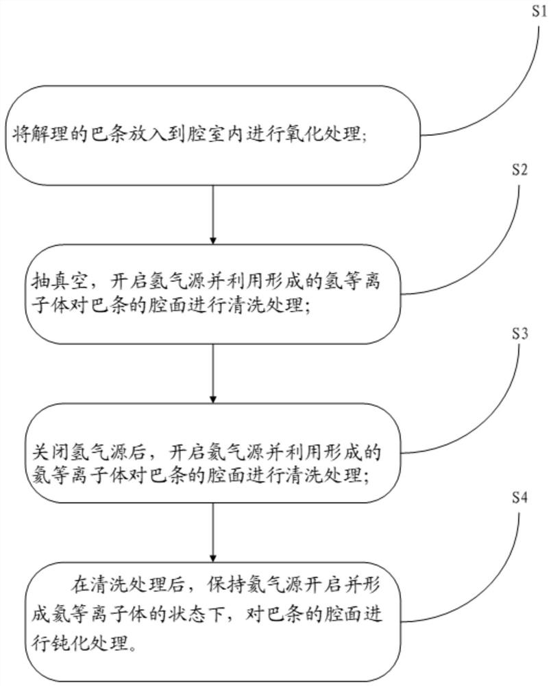
[0028] Such as figure 1 As shown, a kind of passivation method of semiconductor device provided by the present invention comprises the following steps:
[0029] S1: Put the cleaved bars (bars) into the chamber for oxidation treatment;
[0030] S2: Vacuumize, turn on the hydrogen source and use the formed hydrogen plasma to clean the cavity surface of the bar;
[0031] S3: After turning off the hydrogen source, turn on the helium source and use the formed helium plasma to clean the cavity surface of the bar;
[0032] S4: After the cleaning treatment, passivation treatment is performed on the cavity surface of the bar while keeping the helium gas source turned on and forming a helium plasma.
[0033] In the passivation method of the semiconductor device provided by this embodiment, before the bar is cleaned, the bar is oxidized in an oxygen environment, so that the thickness of the oxide layer on the cavity surface of the bar can be made uniform, and the bar can be avoided Cl...
PUM
 Abstract
Description
Claims
Application Information