Thin film uniform deposition and high-precision patterning method based on liquid-phase MXene material and large-scale preparation method of photoelectric device

A technology of optoelectronic devices and material thin films, which is applied in the fields of electrical solid devices, semiconductor/solid device manufacturing, photovoltaic power generation, etc., can solve the problems of low processing precision and poor uniformity, and achieve the effect of high resolution and good photoelectric detection performance

Active Publication Date: 2021-05-07
INST OF METAL RESEARCH - CHINESE ACAD OF SCI
View PDF3 Cites 1 Cited by
  • Summary
  • Abstract
  • Description
  • Claims
  • Application Information

AI Technical Summary

Problems solved by technology

However, the current thin film preparation, high-resolution micro- and nano-scale processing technology has disadvantages such as poor uniformity and low processing precision, which limits the wide application of MXene in the field of microelectronics.

Method used


Image

  • Thin film uniform deposition and high-precision patterning method based on liquid-phase MXene material and large-scale preparation method of photoelectric device
  • Thin film uniform deposition and high-precision patterning method based on liquid-phase MXene material and large-scale preparation method of photoelectric device
  • Thin film uniform deposition and high-precision patterning method based on liquid-phase MXene material and large-scale preparation method of photoelectric device

Examples


Embodiment Construction

[0050] In specific implementation process, the present invention is based on liquid phase MXene (such as: Ti 3 C 2 T x 、Ti 2 CT x etc.) uniform deposition of thin films of suspensions, high-precision patterning and large-scale preparation methods of photoelectric devices, through photolithography-dry etching process, the method of preparing patterned MXene material thin films and MXene-based photodetectors is as follows:

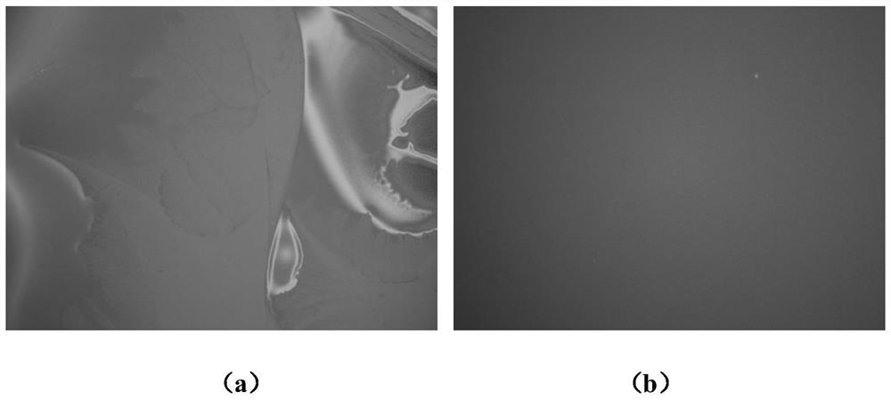
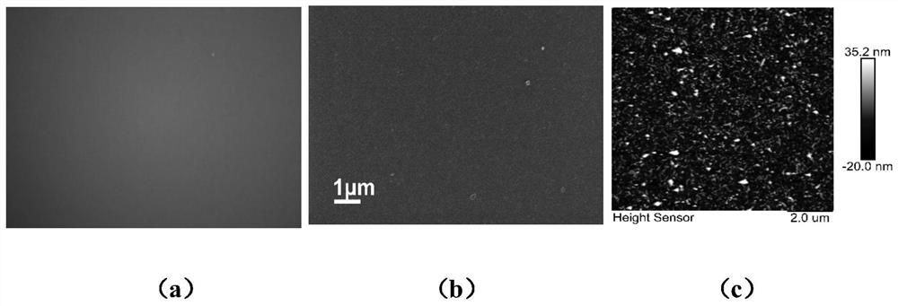
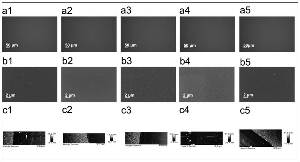
[0051] (1) It is necessary to verify the influence of suspension concentration, spin coating speed and spin coating time on the film formation effect during the preparation of MXene material thin film by spin coating MXene material suspension. First determine the concentration of the MXene material suspension and the spin-coating time, prepare different MXene material films by changing the speed of the homogenizer, and then control the other two parameters at a time to optimize the film-forming effect. The film formation effect was characterized by optic...


PUM

PropertyMeasurementUnit
thicknessaaaaaaaaaa
thicknessaaaaaaaaaa
thicknessaaaaaaaaaa

Abstract

The invention relates to the field of research, development and application of a novel MXene-based photoelectric detector, in particular to a method for uniformly depositing a thin film based on a liquid-phase MXene material, high-precision patterning and preparing a photoelectric device on a large scale. The method comprises the following steps: spin-coating an MXene material suspension through a spin coater, and preparing a uniform MXene material film on a silicon wafer; and realizing the high-precision patterning of the MXene material thin film by adopting a photoetching-dry etching process. The MXene-based photoelectric detector is composed of a silicon substrate, an electrode, a semiconductor layer, a transparent conductive film layer and the like, the electrode, the semiconductor layer, the transparent conductive film layer and the like are arranged on the silicon substrate, the semiconductor layer is made of n-type silicon formed by doping, the transparent conductive film layer is made of MXene materials, and the electrode is formed by compounding a Ti layer and an Au layer. According to the invention, the patterning of the large-area MXene material film is realized by using a photoetching-dry etching process, so that the high-resolution MXene-based photoelectric detector is constructed, and the MXene-based photoelectric detector has good photoelectric performance and long cycle life.

Description

technical field [0001] The invention relates to the field of research and development and application of new MXene-based photodetectors, specifically a method for uniform deposition of thin films based on liquid-phase MXene materials, high-precision patterning of photolithography-dry etching processes, and large-scale preparation of photoelectric devices. Background technique [0002] The two-dimensional material MXene is an important derivative of MAX phase ceramics. MAX phase ceramics is a general term for a class of ternary layered carbonitrides, and its general chemical formula can be expressed as M n+1 AX n (n=1, 2, 3), where M refers to the former transition group metal elements (mainly concentrated in the third, fourth, fifth, and sixth subgroups), A mainly refers to the third and fourth main group elements, and X refers to carbon or nitrogen Elements (for example, Nb 4 AlC 3 、Ti 3 AlC 2 、Ti 3 SiC 2 or Ti 2 AlN, etc.) [1] . MXene mainly uses fluorine-contai...

Claims


Application Information

Patent Timeline
Patent Type & Authority Applications(China)
IPC IPC(8): H01L51/48H01L51/42
CPCH10K71/12H10K30/00Y02E10/549
Inventor 孙东明李波朱钱兵崔聪王晓辉
Owner INST OF METAL RESEARCH - CHINESE ACAD OF SCI
Why Eureka
Try Eureka