
Polymerization curing device and preparation method for preparing polyimide patterned film

A technology for preparing polyimide and thin films, which is applied in the manufacture of semiconductor/solid-state devices, electrical components, circuits, etc., can solve the problems of limiting the density of packaging and wiring, deformation of the three-dimensional topography of the film, and changing the topography integrity of the patterned film.

Pending Publication Date: 2021-05-11
杭州晶通科技有限公司
View PDF0 Cites 0 Cited by
  • Summary
  • Abstract
  • Description
  • Claims
  • Application Information

AI Technical Summary

Problems solved by technology

[0004] Purpose of the invention: The purpose of the present invention is to solve the problem that the existing polyimide patterned film preparation method is to directly heat up and cool down to solidify the current pattern, which will cause a slight deformation of the three-dimensional shape of the patterned film and change the pattern. The integrity of the thin film morphology, and further when high-density packaging is carried out, that is, when the wiring spacing is relatively small, it will greatly limit the density of packaging wiring, thus affecting the integrity of the packaging miniaturization

Method used


Image

  • Polymerization curing device and preparation method for preparing polyimide patterned film
  • Polymerization curing device and preparation method for preparing polyimide patterned film
  • Polymerization curing device and preparation method for preparing polyimide patterned film

Examples


Embodiment 1

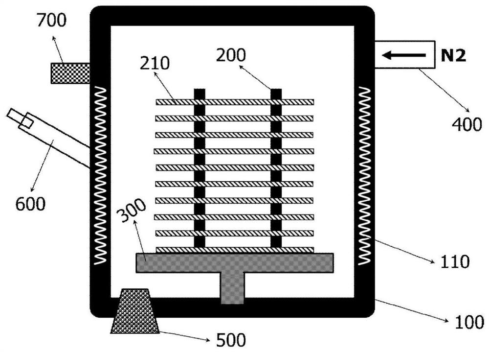
[0035] Such as figure 1 As shown, a polyimide patterned film preparation polymerization curing device, including a cavity 100, on the cavity 100 can be completely isolated from the outside world can be closed door (not shown), the cavity 100 side wall pre-prepared A number of cooling circulating water pipes 110 are buried, and a lifting platform 300 is provided in the cavity 100. A wafer support 200 is provided on the lifting platform 300. The wafer support 200 is provided with a plurality of heating plates that can individually heat the wafer along the vertical direction. 210, the cavity 100 is also provided with a nitrogen gas inlet 400, an air pressure detection device 700, a temperature detection device 600, and a vacuum pump 500, the temperature detection device 600 is a temperature sensor, and the detection direction of the temperature sensor is directed toward any wafer The heating plate 210 on the support 200.

[0036] A nitrogen inlet and a vacuum pump connected to t...

Embodiment 2

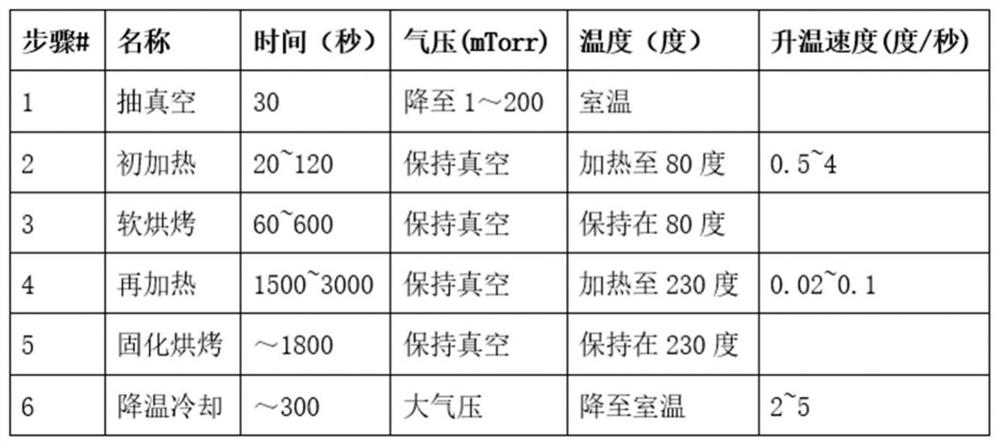
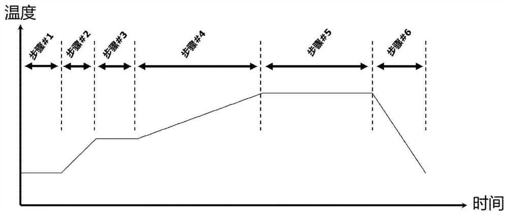
[0047] Such as Figure 1 to Figure 4 Shown, a kind of preparation method of polyimide patterned film comprises the following steps:

[0048] 1) The manipulator clamps and transports multiple wafers to each heating plate 210 in the cavity 100;

[0049] 2) Close the sealable door, and vacuumize the cavity 100, so that the air pressure in the cavity 100 reaches a vacuum state of the order of mTorr;

[0050] 3) heating the cavity 100 at a rate of 0.5-4°C / s to 80°C;

[0051] 4) The cavity 100 is kept at 80°C for 60-600s;

[0052] 5) heating the cavity 100 at a rate of 0.02-0.1°C / s to 230°C;

[0053] 6) The cavity 100 is kept at 230°C for 1800s;

[0054] 7) Cool down the cavity 100 at a rate of 2-5° C. / s to room temperature.

[0055] In step 2) to step 6), the vacuum state of mTorr level is always maintained in the cavity 100 .

[0056] In step 2) to step 6), while the nitrogen generator is supplying nitrogen, the vacuum pump 500 is turned on at the same time to evacuate, so t...


PUM


Abstract

The invention discloses a polymerization curing device for preparing a polyimide patterned film. The device comprises a cavity, a closable door which can be completely isolated from the outside is arranged on the cavity, a plurality of cooling circulating water pipes are pre-buried in the side wall of the cavity, a lifting platform is arranged in the cavity, and a wafer bracket is arranged on the lifting platform. The wafer bracket is provided with a plurality of heating plates capable of independently heating wafers in the vertical direction, the cavity is further provided with a nitrogen inlet, an air pressure detection device, a temperature detection device and a vacuum pump, the temperature detection device is a temperature sensor, and the detection direction of the temperature sensor faces any heating plate on the wafer bracket in the inclined downward direction. The invention also discloses a preparation method of the polyimide patterned film. By adopting the design scheme of the invention, polymerization and curing of the polyimide film are completed through a vacuum gradient heat treatment method, so that the patterned polyimide film after photoetching can still keep a regular three-dimensional morphology.

Description

technical field [0001] The invention relates to the technical field of semiconductor packaging, in particular to a polymerization curing device and a preparation method for preparing a patterned polyimide film. Background technique [0002] With the development trend of high integration, miniaturization and portability of semiconductor chip packaging, the density of packaging wiring is getting higher and higher. In order to have higher density wiring on the same packaging area, the wiring line width and line spacing need to be drastically reduced. In the field of advanced packaging, the line width and line spacing of wiring are often reduced to 2-5um or even smaller. [0003] In advanced packaging of semiconductor chips (such as wafer-level packaging, fan-out packaging), the wiring layer is composed of a patterned polyimide dielectric layer and a metal embedded in it. The polyimide dielectric layer pattern The precision and density of the optimization determine the density...

Claims


Application Information

Patent Timeline
IPC IPC(8): H01L21/67
CPCH01L21/67109H01L21/67248H01L21/67253
Inventor 王新蒋振雷
Owner 杭州晶通科技有限公司
Learn More