Chip design optimization system and method based on dynamic unbalanced clock

A technology of chip design and optimization methods, applied in computer-aided design, computing, special data processing applications, etc.

Active Publication Date: 2021-05-18
上海芷锐电子科技有限公司
View PDF6 Cites 1 Cited by
  • Summary
  • Abstract
  • Description
  • Claims
  • Application Information

AI Technical Summary

Problems solved by technology

[0003] Aiming at the shortage of balanced clock tree in the existing chip design and implementation process, the present invention proposes a chip design optimiz

Method used


Image

  • Chip design optimization system and method based on dynamic unbalanced clock
  • Chip design optimization system and method based on dynamic unbalanced clock
  • Chip design optimization system and method based on dynamic unbalanced clock

Examples


Embodiment Construction

[0044] The chip design optimization system and method based on the dynamic unbalanced clock of the present invention will be further described in detail below in conjunction with the accompanying drawings and specific embodiments.

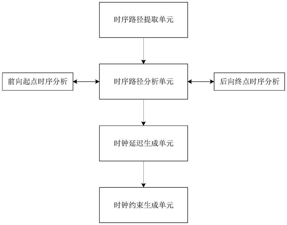
[0045] Such as figure 1 As shown, a chip design optimization system based on a dynamic unbalanced clock includes sequentially connected timing path extraction unit, timing path analysis unit, clock delay generation unit and clock constraint generation unit.

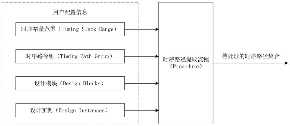
[0046] The timing path extracting unit is used to extract the timing paths to be analyzed that meet the requirements from the designed timing paths, and send them to the timing path analysis unit.

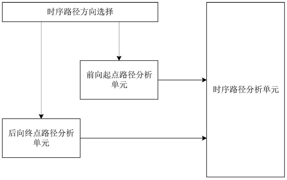
[0047] combine image 3 , the timing path analysis unit includes a forward start timing analysis unit and a backward end timing analysis unit, the forward start timing analysis unit is used to analyze and extract the timing state when the starting point of the timing path is taken as the end point...


PUM


Abstract

The invention provides a chip design optimization system and method based on a dynamic unbalanced clock. In a designed synthesis stage, a designed time sequence path is analyzed, clock delay of a time sequence unit is analyzed and dynamically adjusted according to a current time sequence result, and a clock delay result is transmitted to subsequent steps of a chip design implementation process, so that an unbalanced clock tree structure is synthesized according to requirements during clock tree synthesis. The delay of the whole leaf node clock network is dynamically adjusted in the synthesis and layout wiring stage in the chip design implementation process, so that the purpose of quickly converging the time sequence is achieved. Due to the fact that the dynamic unbalanced clock network is used, the time sequence path of chip design has more time sequence allowance, a chip implementation tool can better optimize the whole designed time sequence, the path with tense time sequence does not need more complex optimization, and therefore the area of the whole design is reduced, power consumption is reduced, and cost is reduced. The achievable clock speed of the design is improved, and the design performance is improved.

Description

technical field [0001] The invention belongs to the technical field of integrated circuits, and in particular relates to a chip design optimization system and method based on a dynamic unbalanced clock. Background technique [0002] The integrated circuit design and implementation process includes a synthesis stage and a layout and routing stage. In the synthesis stage, in the traditional process, the clock is ideal, and the delay from the clock source to different registers is the same, only from the timing constraints of the design. Use the clock uncertainty (Clock Uncertainty) to be constrained. This kind of constraint is relatively arbitrary, and it is difficult to meet the design constraint requirements for some timing paths with relatively tight timing requirements. However, in the implementation process, if such a timing path has a timing margin in the forward timing path or the backward timing path, the timing path can be made Meet the final design requirements. T...

Claims


Application Information

Patent Timeline
IPC IPC(8): G06F30/337G06F30/3312G06F30/327G06F30/396
CPCG06F30/337G06F30/3312G06F30/327G06F30/396G06F2119/12
Inventor 袁肖华于威阙诗璇
Owner 上海芷锐电子科技有限公司
Why Eureka
Try Eureka