

Silicon wafer processing device and processing technology for chip preparation
A technology for processing devices and silicon wafers, which is applied in semiconductor/solid-state device manufacturing, electrical components, circuits, etc., can solve problems such as temperature softening deformation, clamping device offset, and lack of silicon wafer 4, so as to prevent softening and deformation Effect
- Summary
- Abstract
- Description
- Claims
- Application Information
AI Technical Summary
Problems solved by technology
Method used
Image

Examples
Embodiment 1
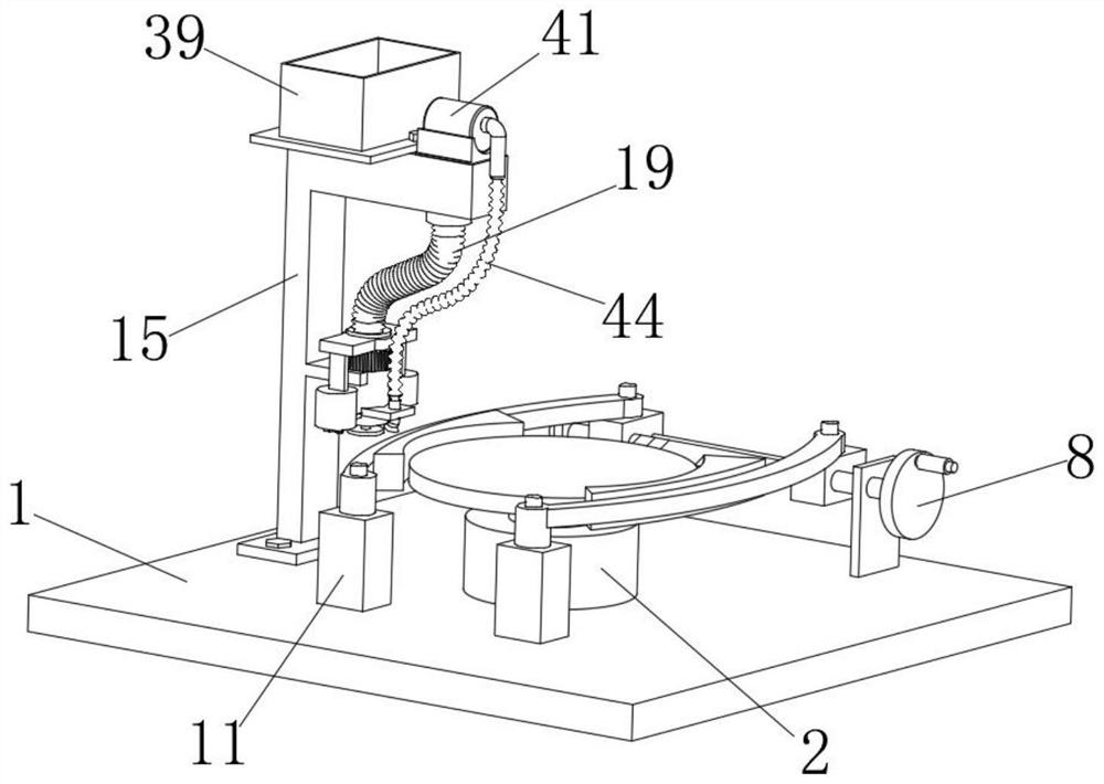
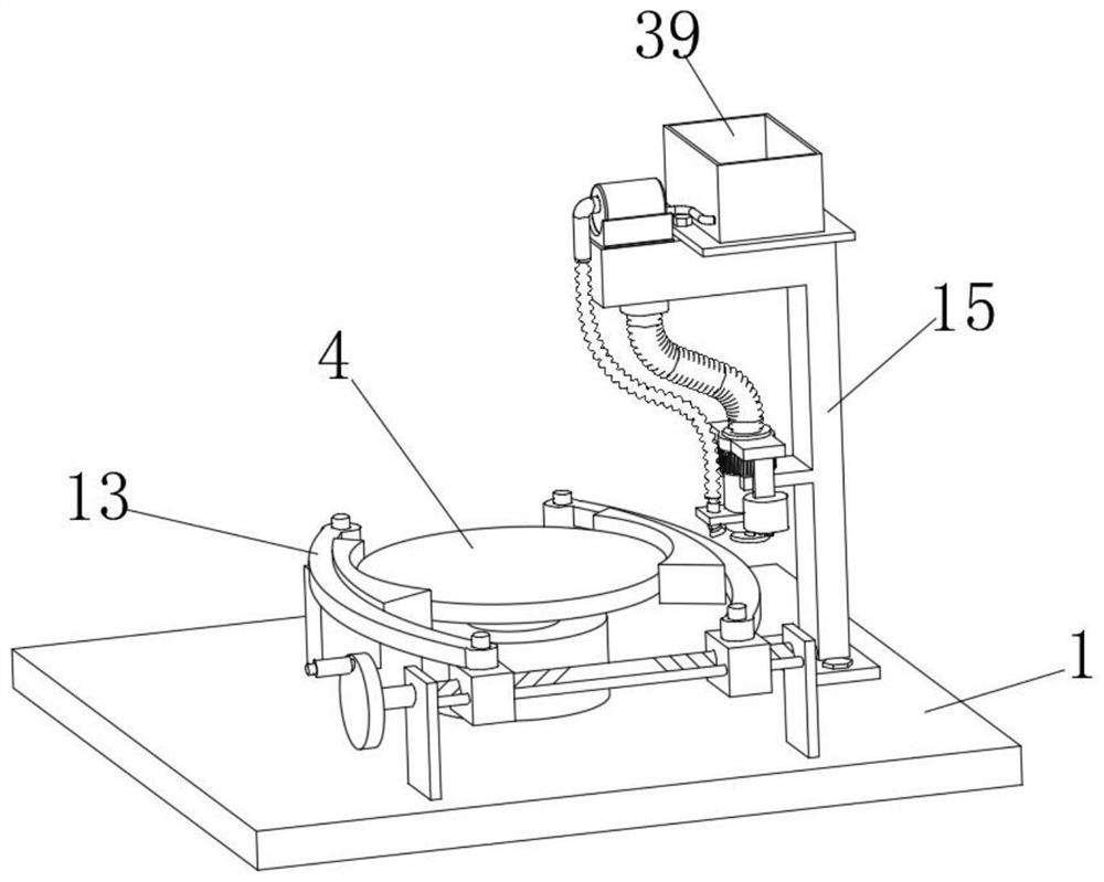
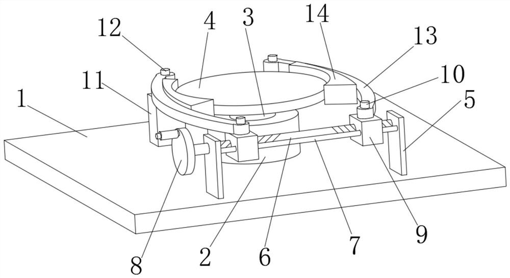
[0034] In a typical implementation of the present application, such as Figure 1-8As shown, a silicon wafer processing device for chip preparation includes a base plate 1, a support column 2 is fixedly connected to the top of the base plate 1, a support platform 3 is fixedly connected to the top of the support column 2, and a silicon wafer is arranged on the top of the support platform 3 4. The top of the bottom plate 1 is fixedly connected with two fixed plates 5, and the side walls of the two fixed plates 5 are provided with rotating holes, and the same two-way threaded rod 6 is connected to the rotating socket in the two rotating holes. The two ends of the rod 6 pass through the rotating holes respectively, and extend to the outsides of the two fixed plates 5. One end of the two-way threaded rod 6 is fixedly connected with a hand wheel 8, and two sliding blocks 9 are screwed on the two-way threaded rod 6. Perforations are provided on one side wall of each sliding block 9, a...
PUM
 Abstract
Description
Claims
Application Information