SGTMOSFET device and manufacturing method

A technology of devices and conditions, applied in semiconductor/solid-state device manufacturing, semiconductor devices, electrical components, etc., can solve problems such as ugly appearance and influence on device reliability, so as to reduce the influence of warpage, improve product yield, and reduce stress Effect

Pending Publication Date: 2021-05-28
NANTONG SANRISE INTEGRATED CIRCUIT CO LTD
View PDF0 Cites 2 Cited by
  • Summary
  • Abstract
  • Description
  • Claims
  • Application Information

AI Technical Summary

Problems solved by technology

This increases the device's input capacitance (Ciss), which is the parallel capacitance of the gate-to-source capacitance (Cgs) and the gate-to-drain capacitance (Ggd)
And the appearance has become ugly
The shape of the polysilicon gate 6a may form some sharp corners, which will cause the device to form a spike in the electric field, which will also have some impact on the reliability of the device

Method used


Image

  • SGTMOSFET device and manufacturing method
  • SGTMOSFET device and manufacturing method
  • SGTMOSFET device and manufacturing method

Examples


Embodiment Construction

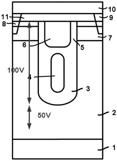
[0090] Such as Figure 5 Shown is a schematic structural diagram of the SGTMOSFET device of the embodiment of the present invention; the withstand voltage of the SGTMOSFET device of the embodiment of the present invention is above 150V. A gate structure is formed in the gate trench.

[0091] The gate trench is formed in the first epitaxial layer 2 of the first conductivity type. The first epitaxial layer 2 is formed on the heavily doped semiconductor substrate 1 of the first conductivity type.

[0092] A bottom oxide layer 3 is formed on the inner surface of the gate trench. The thickness of the bottom oxide layer 3 is required to meet the withstand voltage condition of 150V or more. The thicker the bottom oxide layer 3 is, the lower the bottom oxide layer is. 3 has a higher withstand voltage; the bottom oxide layer 3 is composed of a thermal oxide layer and a CVD-deposited oxide layer, so as to meet the stress condition of the bottom oxide layer 3 .

[0093] The bottom oxi...


PUM

PropertyMeasurementUnit
depthaaaaaaaaaa
thicknessaaaaaaaaaa
thicknessaaaaaaaaaa

Abstract

Dsiclosed is an SGTMOSFET device and a manufacturing method. A bottom oxide layer and source polycrystalline silicon of a grid structure are located at the bottom of a grid groove, the thickness of the bottom oxide layer meets the requirement for voltage resistance of 150V or above, the top of the grid groove is filled with a top oxide layer completely formed through CVD deposition, a polycrystalline silicon grid is formed in a top sub-groove formed by etching the top oxide layer, the width of the top sub-groove meets the requirement for filling the polycrystalline silicon grid, and when the depths of the two side faces of the top sub-groove are the same, the depths of the two side faces of the polycrystalline silicon grid are the same. The invention further provides a manufacturing method of an SGTMOSFET device. According to the invention, under the condition of ensuring that the bottom oxide layer realizes the withstand voltage of more than 150V, the polycrystalline silicon grid with a left-right structure is adopted, so that the width of the polycrystalline silicon grid can realize good and low-difficulty filling of the polycrystalline silicon grid, and the depths of the two side surfaces of the polycrystalline silicon grid can be ensured to be consistent; therefore, the increase of input capacitance can be avoided and the reliability of the device can be improved under the condition of meeting the coverage length of a channel region.

Description

technical field [0001] The invention relates to a method for manufacturing a semiconductor integrated circuit, in particular to a method for manufacturing a Shield Gate Trench (ShieldGate Trench, SGT) MOSFET device. Background technique [0002] Compared with IGBT, MOSFET is a multi-sub device, because there is no minority sub-injection and recombination during the switching process, so its switching speed is fast and it has been widely used. Compared with the traditional planar MOSFET, the trench MOSFET greatly reduces the channel resistance, but the on-resistance of the drift region is proportional to the 2.5th power of the breakdown voltage, which makes the resistance of the drift region become unacceptable. [0003] In order to reduce the on-resistance in the drift region, SGTMOSFET was proposed. SGTMOSFET inserts a vertical field plate in the drift region, and this field plate is connected to the source voltage. In the process of bearing the breakdown voltage, the dr...

Claims


Application Information

Patent Timeline
Patent Type & Authority Applications(China)
IPC IPC(8): H01L29/78H01L29/423H01L21/28H01L21/336
CPCH01L21/28035H01L29/4236H01L29/42364H01L29/42376H01L29/66613H01L29/66666H01L29/7827
Inventor 曾大杰
Owner NANTONG SANRISE INTEGRATED CIRCUIT CO LTD
Why Eureka
Try Eureka