Multi-station probe card and wafer testing method

A probe card and multi-station technology, which is applied in the direction of electronic circuit testing, components of electrical measuring instruments, measuring electricity, etc., can solve the problem of reducing the service life of probe cards, expensive probe cards, and long wafer testing time. and other issues to achieve the effect of improving accuracy and test yield, improving test yield and stability, and stabilizing stitches and test status

Pending Publication Date: 2021-06-01
SINO IC TECH
View PDF0 Cites 0 Cited by
  • Summary
  • Abstract
  • Description
  • Claims
  • Application Information

AI Technical Summary

Problems solved by technology

However, the main problem of this method is that the number of times of preheating is too long and the time is too long, which makes the whole wafer test time too long and the test efficiency is low; Problems may occur at any time due to contact conditions, stitches, etc., resulting in low test yield
But preheating takes time and monitoring of stitches, the efficiency is low and the effect is not ideal
In addition, due to the wafer production process, the surface of the edge area of ​​the wafer is relatively rough. When the probe card is in contact with the pad or bump in the edge area of ​​the wafer, the probes on the probe card are easily worn. And the price of the probe card is relatively expensive. If the probes on the probe card are worn out, it will cause inaccurate tests at other positions and reduce the service life of the probe card.

Method used


Image

  • Multi-station probe card and wafer testing method
  • Multi-station probe card and wafer testing method
  • Multi-station probe card and wafer testing method

Examples


Embodiment Construction

[0033] The specific implementation manner of the present invention will be described in more detail below with reference to schematic diagrams. The advantages and features of the present invention will be more apparent from the following description. It should be noted that all the drawings are in a very simplified form and use imprecise scales, and are only used to facilitate and clearly assist the purpose of illustrating the embodiments of the present invention.

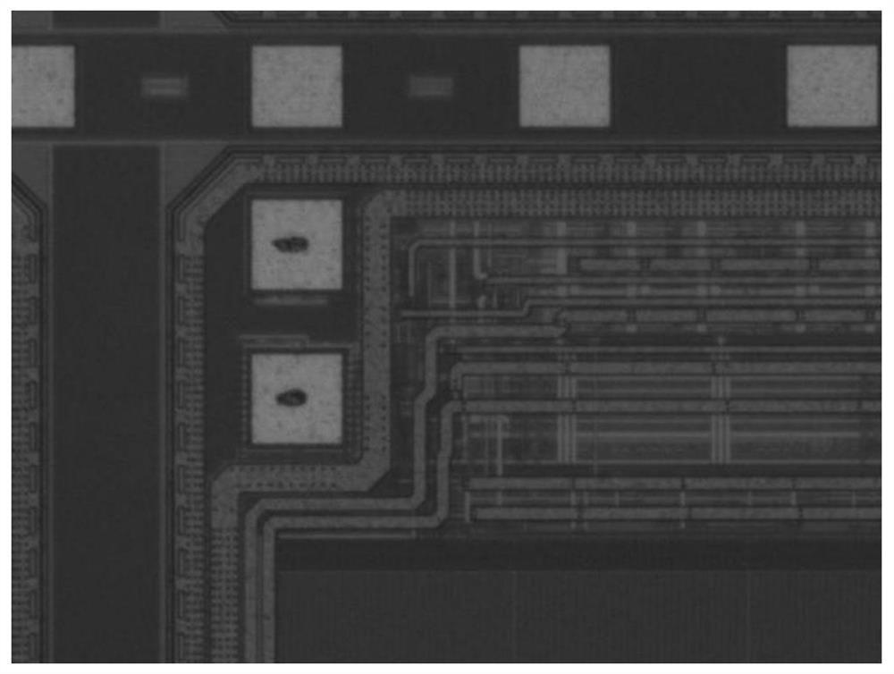
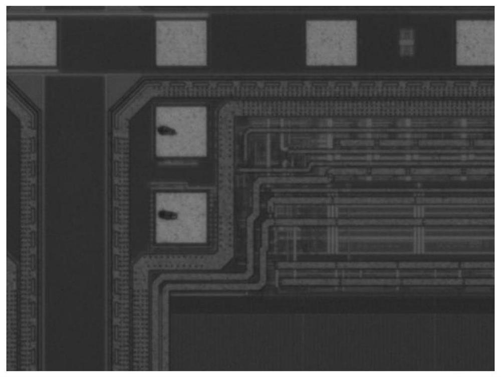
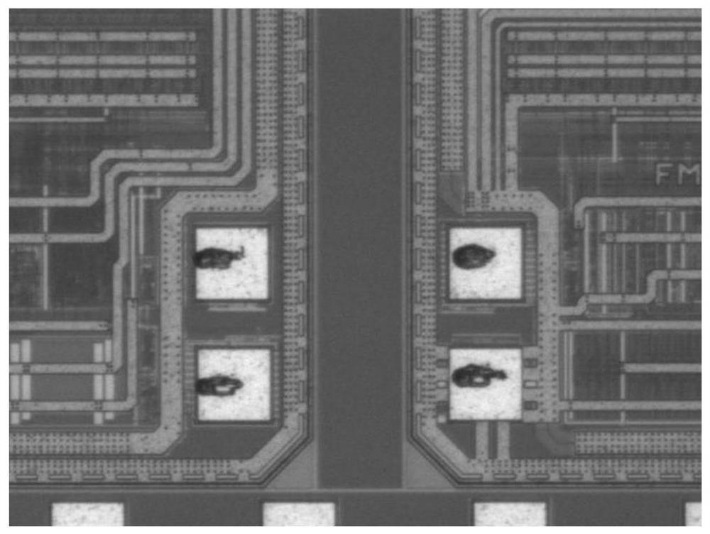
[0034] Image 6 Schematic diagram of the structure of the multi-station probe card provided in this embodiment; Figure 7 The method for the wafer test that this embodiment provides; Figure 8 The MAP diagram under the high temperature test provided for this embodiment. This embodiment provides a multi-station probe card to improve test accuracy and test yield, including a substrate, several probes, a strengthening board and a shielding layer.

[0035] Please refer to Image 6 , wherein the substrate 11 is a p...


PUM


Abstract

The invention provides a multi-station probe card and a wafer testing method. The multi-station probe card comprises: a base plate provided with a plurality of through holes; a reinforcing plate located on the upper surface of the base plate and provided with a heat conducting sheet, wherein the heat conducting sheet is used for conducting external temperature to the base plate; and a plurality of probes circumferentially distributed outside each through hole, wherein one end of each probe is connected with the lower surface of the base plate, the other end of each probe extends outwards from the lower surface of the base plate, and the through holes and the circumferentially distributed probes form a probe station. According to the invention, the test accuracy and the test yield of the wafer can be improved.

Description

technical field [0001] The invention relates to the technical field of semiconductors, in particular to a multi-station probe card and a wafer testing method. Background technique [0002] Wafer testing is an important link in the entire process of integrated circuits. It is an electrical parameter measurement and performance test performed before wafer dicing in order to verify the consistency of integrated circuit design specifications. Wafer testing develops a test plan based on product parameters and performance tests. In the process of formulating a test plan, the processing of test hardware is the most important, mainly including several aspects: test machine, test probe card and test hardware. The tester and the probe station are usually general-purpose machines, and the probe card serves as the core interface between the tester and the device under test on the wafer, which can best reflect the test plan of a product. A typical probe card is usually a printed circuit...

Claims


Application Information

Patent Timeline
Patent Type & Authority Applications(China)
IPC IPC(8): G01R31/28G01R1/04
CPCG01R1/0408G01R31/2806G01R31/2851G01R31/2886
Inventor 罗斌刘远华王锦崔孝叶范文萱季海英
Owner SINO IC TECH
Why Eureka
Try Eureka