Preparation method of silicon carbide epitaxial structure and semiconductor equipment

An epitaxial structure, silicon carbide technology, applied in semiconductor/solid-state device manufacturing, electrical components, circuits, etc., can solve the problems of growth surface defect density device yield decline and other problems, achieve continuous growth, improve yield, and reduce surface defects. Effect

Pending Publication Date: 2021-06-01
CEC COMPOUND SEMICON CO LTD
View PDF6 Cites 2 Cited by
  • Summary
  • Abstract
  • Description
  • Claims
  • Application Information

AI Technical Summary

Problems solved by technology

[0005] Aiming at the deficiencies and defects in the prior art, the present invention provides a method for preparing a silicon carbide epitaxial structure and semiconductor equipment, which are used to solve the influence of P-type dopants on the growth of N-type epitaxial layers in the silicon carbide epitaxial structure and surface defects The problem of device yield reduction caused by density

Method used


Image

  • Preparation method of silicon carbide epitaxial structure and semiconductor equipment
  • Preparation method of silicon carbide epitaxial structure and semiconductor equipment

Examples


Embodiment Construction

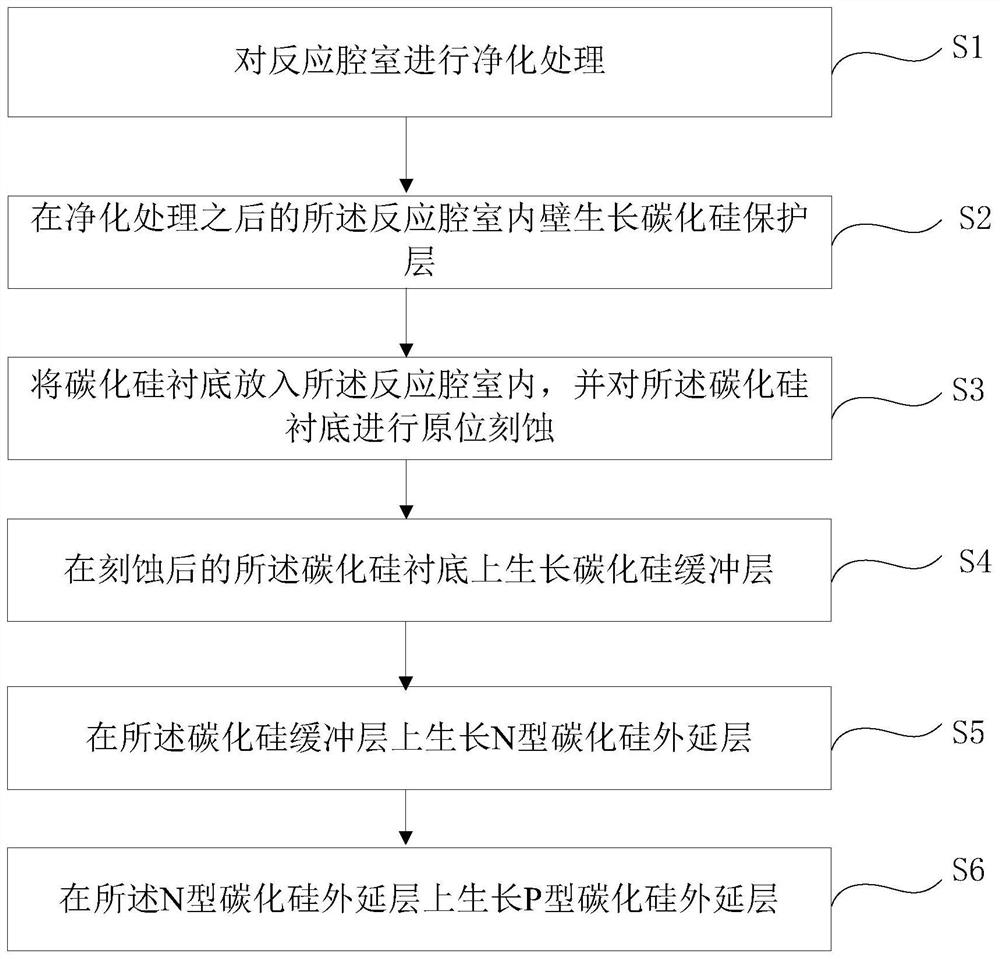
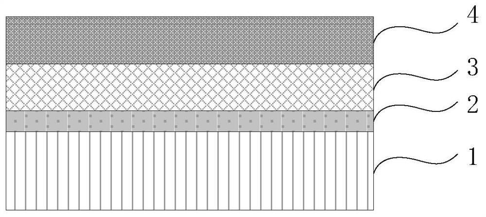
[0031] Embodiments of the present invention are described below through specific examples, and those skilled in the art can easily understand other advantages and effects of the present invention from the content disclosed in this specification. The present invention can also be implemented or applied through other different specific implementation modes, and various modifications or changes can be made to the details in this specification based on different viewpoints and applications without departing from the spirit of the present invention. It should be noted that, in the case of no conflict, the following embodiments and features in the embodiments can be combined with each other. It should also be understood that the terminology used in the embodiments of the present invention is for describing specific implementations, not for limiting the protection scope of the present invention. The test methods for which specific conditions are not indicated in the following example...


PUM

PropertyMeasurementUnit
thicknessaaaaaaaaaa

Abstract

The invention provides a preparation method of a silicon carbide epitaxial structure. The preparation method comprises the following steps: purifying a reaction chamber; growing a silicon carbide protection layer on the inner wall of the reaction chamber after purification treatment; putting a silicon carbide substrate into the reaction chamber, and performing in-situ etching on the silicon carbide substrate; growing a silicon carbide buffer layer on the etched silicon carbide substrate; growing an N-type silicon carbide epitaxial layer on the silicon carbide buffer layer; and growing a P-type silicon carbide epitaxial layer on the N-type silicon carbide epitaxial layer. The preparation method is simple, growth of epitaxial layers of different doping types can be completed in the same chamber, continuous growth of the epitaxial layers of different doping types is achieved, surface defects of a silicon carbide epitaxial structure are reduced, and the yield of silicon carbide devices is improved.

Description

technical field [0001] The invention relates to the technical field of semiconductor materials, in particular to a method for preparing a silicon carbide epitaxial structure and semiconductor equipment. Background technique [0002] Silicon carbide (SiC) semiconductor has excellent characteristics such as large bandgap width, excellent stability, high thermal conductivity, high critical breakdown field strength, high saturation electron drift velocity, etc. It is ideal for high temperature, high frequency, high power and strong radiation power Ideal semiconductor material for electronic devices. Compared with traditional silicon devices, silicon carbide devices can work normally under the electric field strength 10 times that of silicon devices. Due to these superior characteristics of silicon carbide, it has broad application prospects in the fields of chemical industry, aerospace engineering, nuclear power engineering, electronic components and electronic circuits. [00...

Claims


Application Information

Patent Timeline
Patent Type & Authority Applications(China)
IPC IPC(8): H01L21/02
CPCH01L21/02378H01L21/02447H01L21/02496H01L21/02529H01L21/0262
Inventor 周长健潘尧波唐军
Owner CEC COMPOUND SEMICON CO LTD
Why Eureka
Try Eureka