Deep silicon detector module integrated with pre-amplification circuit
A preamplifier circuit and detector technology, applied in the field of detectors, can solve the problems of low definition, large space occupation, and limited resolution of detectors, and achieve the effects of reduced volume and weight, tight arrangement, and wide application prospects
- Summary
- Abstract
- Description
- Claims
- Application Information
AI Technical Summary
Problems solved by technology
Method used
Image
Examples
Embodiment 1
[0051] The invention provides a deep silicon detector module integrating a preamplifier circuit, including at least two detector chips;
[0052] The detector chips are stacked, and the adjacent detector chips are insulated;
[0053] The detector chip is provided with a light-receiving side, the light-receiving side of each detector chip is arranged on the same arc surface, the adjacent detector chips are arranged at an angle, and the angle between the adjacent detector chips is smaller than the set threshold;
[0054] The detector chip includes a sensitive area unit, a preamplification processing chip integrated area unit, a bonding area unit and an opening area unit;
[0055] The sensitive area unit is arranged on the light-receiving side of the detector chip; the sensitive area unit includes a number of silicon microstrips, each silicon microstrip is parallel, and is distributed along the edge of the light-receiving side of the detector chip to the inside of the detector chi...
Embodiment 2
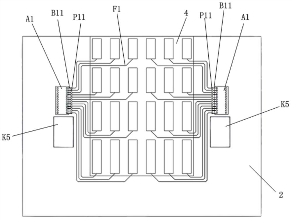
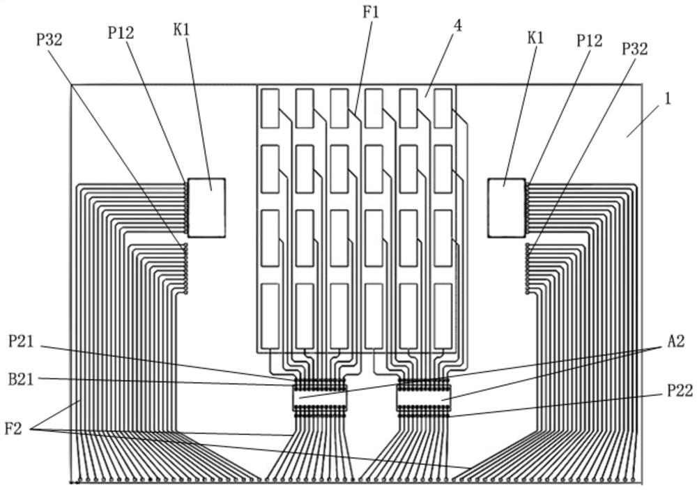
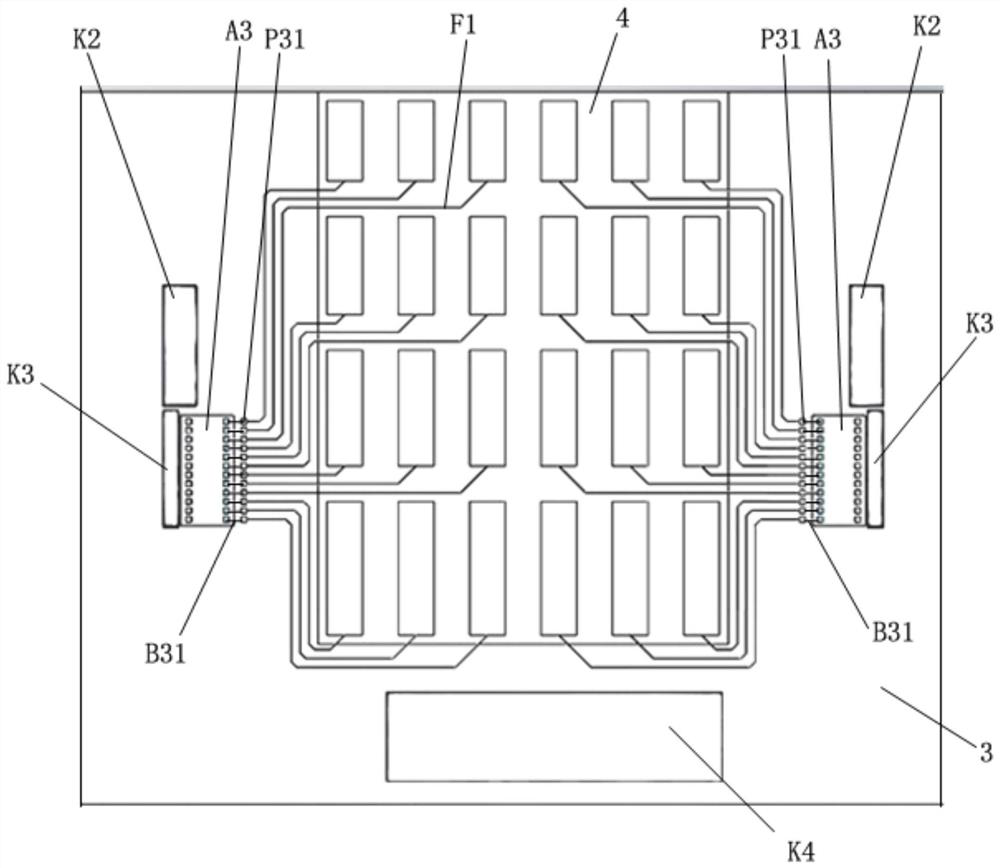
[0088] Such as figure 1 , figure 2 and image 3 As shown, the present invention provides a deep silicon detector module integrating a preamplifier circuit, including three detector chips; the detector chip is divided into a main detector chip and a slave detector chip; wherein, the three detector chips are Master detector chip 1, first slave detector chip 2 and second slave detector chip 3;
[0089] Three detector chips are stacked, wherein the first slave detector chip 2 is located at the bottom layer, the main detector chip 1 is located at the middle layer, and the second slave detector chip 3 is located at the uppermost layer, and the adjacent detector chips are insulated set up;
[0090] The three detector chips are all provided with a light-receiving side, and the light-receiving sides of the three detector chips are arranged on the same arc surface, and the main detector chip 1, the first slave detector chip 2 and the second slave detector chip 3 are all arranged at ...
PUM
| Property | Measurement | Unit |
|---|---|---|
| thickness | aaaaa | aaaaa |
Abstract
Description
Claims
Application Information


