GaN charger control circuit

A charging circuit and control circuit technology, applied in battery circuit devices, current collectors, circuit devices, etc., can solve the problems of low work efficiency, large on-resistance, and high switching loss, and achieve simplified specification design, small oscillation, and switching loss. and EMI good effect

Active Publication Date: 2021-06-08
HUNAN JUSHEN ELECTRONICS CO LTD
View PDF13 Cites 4 Cited by
  • Summary
  • Abstract
  • Description
  • Claims
  • Application Information

AI Technical Summary

Problems solved by technology

[0006] The present invention provides a GaN charger control circuit to solve the problem of high switching loss, large on-resistance, low work efficiency, and low cost in the prior art. The case of tall, bulky problems

Method used


Image

  • GaN charger control circuit
  • GaN charger control circuit
  • GaN charger control circuit

Examples


Embodiment Construction

[0063] The preferred embodiments of the present invention will be described below in conjunction with the accompanying drawings. It should be understood that the preferred embodiments described here are only used to illustrate and explain the present invention, and are not intended to limit the present invention.

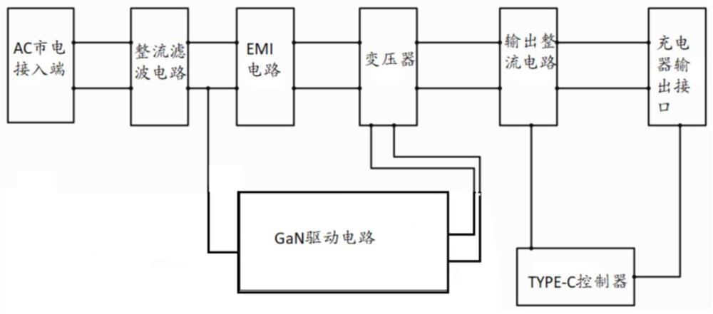
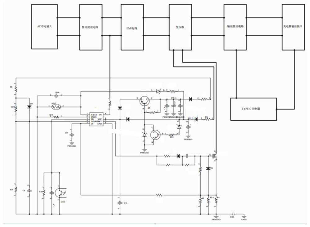
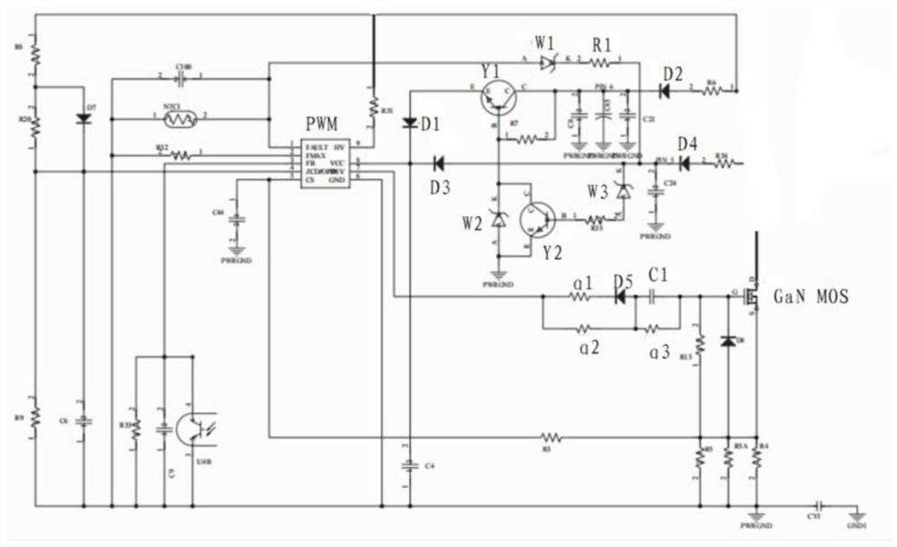
[0064] The invention provides a GaN charger control circuit. It includes: a charging circuit and a GaN driving circuit, the charging circuit is electrically connected to the GaN driving circuit; wherein the GaN driving circuit includes a PWM controller and a GaN MOS tube; wherein the PWM controller is used to control the charging circuit Operating frequency; the GaN MOS transistor is used to drive the charging circuit to start according to the operating frequency. The beneficial effect of the present invention is that: the present invention is a GaN (third-generation device) gallium nitride with a high-frequency and high-efficiency PWM drive chip control circuit, wh...


PUM


Abstract

The invention provides a GaN charger control circuit, which comprises: a charging circuit and a GaN driving circuit, and the charging circuit is electrically connected with the GaN driving circuit; wherein the GaN driving circuit comprises a PWM (Pulse Width Modulation) controller and a GaN MOS (Metal Oxide Semiconductor) tube; wherein the PWM controller is used for controlling the operation frequency of the charging circuit; and the GaN MOS tube is used for driving the charging circuit to start according to the operation frequency. The invention has the beneficial effects that: GaN (third-generation device) gallium nitride is matched with a high-frequency and high-efficiency PWM driving chip control circuit, lower driving loss is realized, lower Miller effect/lower switching loss are achieved, oscillation is small, and the corresponding switching loss and EMI are better. The gallium nitride technology is applied to a high-power charger, so that the conversion efficiency is higher and is up to 93% or above, the switching speed is higher, the working frequency is 100-500KHZ or above, and the purposes of high efficiency and energy conservation are achieved. By adopting the gallium nitride technology, the specification design of the element can be simplified, and a smaller size appearance can be achieved.

Description

technical field [0001] The invention relates to the technical field of charging, in particular to a GaN charger control circuit. Background technique [0002] At present, with the development of technology, electronic products and devices have been widely used, and with the popularization of portable electronic products, chargers with high power, high density and high efficiency are the future trend. [0003] In order to meet the needs of high-power and high-efficiency chargers, the following control schemes are usually used on the market to solve the needs: [0004] 1>PWM controller + MOSFET metal oxide semiconductor field effect tube switching loss is high and the on-resistance is large; the working efficiency is low. [0005] 2>PFC+PWM controller+MOSFET metal-oxide-semiconductor field-effect transistor has higher efficiency, but high cost and large volume. Contents of the invention [0006] The present invention provides a GaN charger control circuit, which is u...

Claims


Application Information

Patent Timeline
Patent Type & Authority Applications(China)
IPC IPC(8): H02J7/10H02M1/08H02M1/36H02M1/44
CPCH02J7/06H02M1/08H02M1/36H02M1/44Y02B70/10
Inventor 赵智星冷昭君詹海峰杨譓鹏
Owner HUNAN JUSHEN ELECTRONICS CO LTD
Why Eureka
Try Eureka