Stacked packaging structure and packaging method
A packaging structure and packaging method technology, applied in the direction of semiconductor/solid-state device components, semiconductor devices, electrical components, etc., can solve the problems of cracks, delamination at the interface of three-layer stack structure, and different degrees of expansion or contraction. , to increase the contact area, prevent delamination or cracks, and increase the adhesion
- Summary
- Abstract
- Description
- Claims
- Application Information
AI Technical Summary
Problems solved by technology
Method used
Image
Examples
Embodiment 1
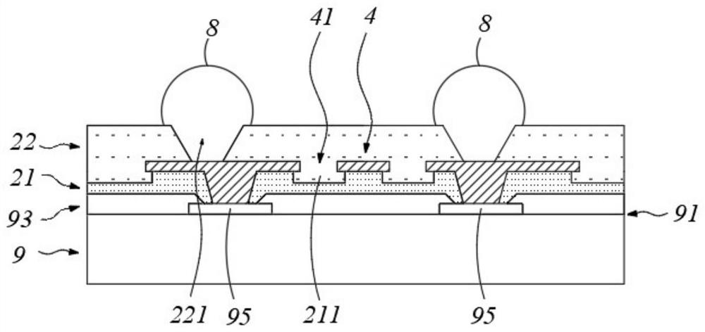
[0057] Such as figure 1 As shown, the active surface 91 of the chip 9 has a three-layer stacked structure. The active surface 91 is also provided with a metal pad 95 and a protection layer 93 . The metal pad 95 is exposed outside the protection layer 93 .
[0058] The first dielectric layer 21 is disposed above the active surface 91 of the chip 9 ; the first dielectric layer 21 is also provided with an opening to expose at least part of the metal pad 95 .
[0059] The redistribution layer 4 is disposed above the first dielectric layer 21; the redistribution layer 4 is electrically connected to the exposed part of the metal pad 95 through the opening provided by the first dielectric layer 21; the redistribution layer 4 is provided with a first metal The layer opening 41 , the first metal layer opening 41 penetrates the redistribution layer 4 along the material thickness direction, exposing at least part of the surface of the first dielectric layer 21 .
[0060] The surface of ...
Embodiment 2
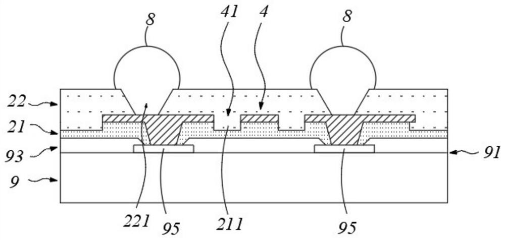
[0063] Such as figure 2 As shown, similarly, the active surface 91 of the chip 9 has a three-layer stacked structure, and the active surface 91 is also provided with a metal pad 95 and a protection layer 93 , and the metal pad 95 is exposed outside the protection layer 93 .
[0064] Different from the first embodiment, in this embodiment, the first groove 211 and the first metal layer have the same width, that is, the boundary of the first groove 211 is flush with the boundary of the first metal layer, and both can be simultaneously It is formed by laser or etching, and the processing is convenient and the process is simple.
Embodiment 3
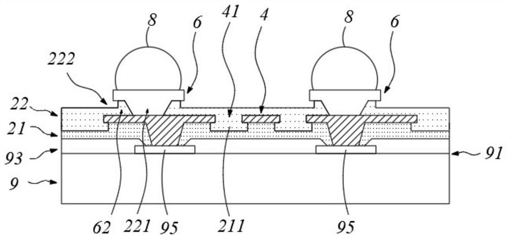
[0066] Such as image 3 As shown, similarly, the active surface 91 of the chip 9 has a three-layer stacked structure, and the active surface 91 is also provided with a metal pad 95 and a protection layer 93 , and the metal pad 95 is exposed outside the protection layer 93 .
[0067] The difference from the first embodiment is that in this embodiment, an under-ball metal layer 6 is formed in the second dielectric layer opening 221, and after the under-ball metal layer 6 passes through or passes through the second dielectric layer opening 221, it is connected with The lower redistribution layer 4 is electrically connected.
[0068] Metal solder balls such as solder balls 8 are formed by soldering on the UBM layer 6 , so that the solder balls 8 are electrically connected to the UBM layer 6 .
PUM
 Abstract
Description
Claims
Application Information
 - R&D
- Intellectual Property
- Life Sciences
- Materials
- Tech Scout
- Unparalleled Data Quality
- Higher Quality Content
- 60% Fewer Hallucinations
Browse by: Latest US Patents, China's latest patents, Technical Efficacy Thesaurus, Application Domain, Technology Topic, Popular Technical Reports.
© 2025 PatSnap. All rights reserved.Legal|Privacy policy|Modern Slavery Act Transparency Statement|Sitemap|About US| Contact US: help@patsnap.com


