

Gallium nitride device reliability testing device and testing method
A technology for gallium nitride devices and test equipment, which is applied in single semiconductor device testing, measurement equipment, climate sustainability, etc., can solve the problem of limited test frequency and duty cycle, high system power consumption, and limited multi-dimensional accelerated testing and other problems, to achieve the effect of reducing system test power consumption and high flexibility
- Summary
- Abstract
- Description
- Claims
- Application Information
AI Technical Summary
Problems solved by technology
Method used
Image

Examples
Embodiment 1
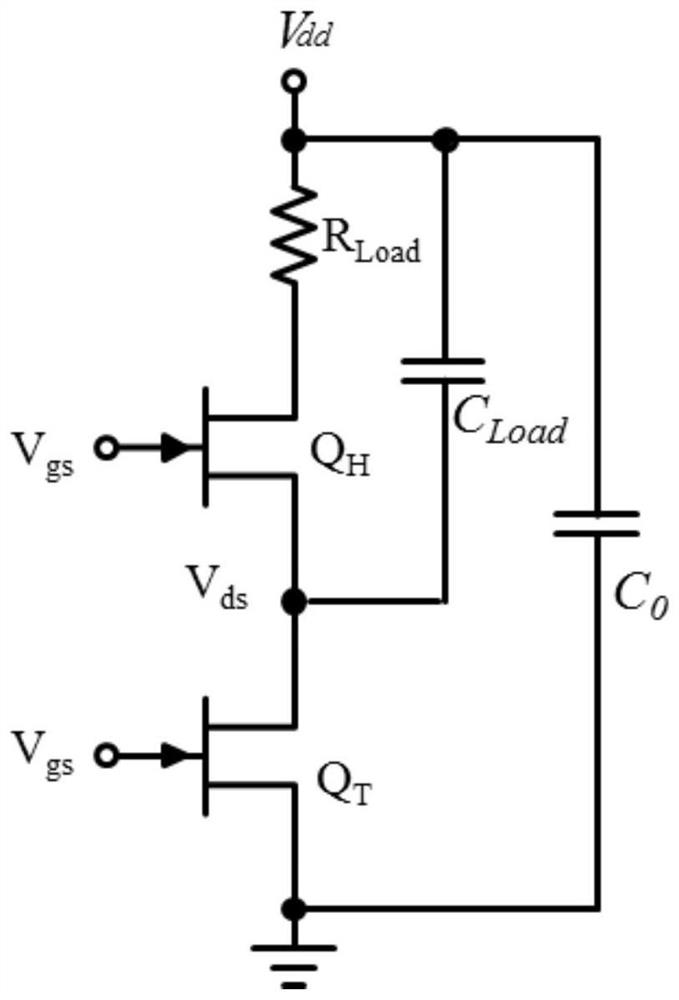
[0036] Reference attached figure 1 , the gallium nitride device reliability testing device of the embodiment of the present invention, comprises load resistance R load , load capacitance C load , the first semiconductor switching device Q H , in the embodiment of the present invention, the first semiconductor switching device Q H is a GaN device; the load resistor R load Connect one end to the DC power supply V dd , the load resistor R load The other end is connected to the first GaN device Q H the drain of the first GaN device Q H The sources of are respectively connected to the GaN device under test Q T The drain, load capacitance C load at one end, the load capacitance C load The other end is connected to the DC power supply V dd , the source of the gallium nitride device to be tested is grounded; the first gallium nitride device Q H The gate of is connected to the first pulse generator, and the gallium nitride device Q to be tested is T The gate of is connected...
Embodiment 2
[0048] In the embodiment of the present invention, the present invention also discloses a method for testing the reliability of GaN devices, including the following steps:
[0049] Step 1, measure the on-resistance of the GaN device to be tested, denoted as Ron;
[0050] Step 2, connect the GaN device to be tested to the GaN reliability test device, and Step 3, set the DC power supply V dd , the duty cycle of the pulse signal output by the first pulse generator, and the duty cycle of the pulse signal output by the second pulse generator;
[0051] Step 4, the gallium nitride reliability test device is placed and operated at the set test temperature;
[0052] Step 5: After the gallium nitride device to be tested has been operated by the reliability device for a period of time, take out the gallium nitride device to be tested, and measure its on-resistance, which is denoted as R'on;
[0053] Step 6, change the on-resistance of the GaN-to-be-tested device before and after the Ga...
Embodiment 3
[0069] The GaN device reliability testing method in Embodiment 2 of the present invention is the same as Embodiment 2. The difference from Embodiment 2 is that in the embodiment of the present invention, the upper transistor (the first semiconductor switching device) of the half-bridge circuit is extended ) pulse width, as attached Figure 5 As shown, the pulse current width flowing through the GaN device to be tested is further adjusted to realize the multi-switch test mode. When the pulse signal output by the second pulse generator changes from low level to high level, the first pulse The pulse signal output by the generator remains high.
[0070] The first GaN device Q H and the GaN device under test Q T A certain overlap time is added to the driving signal in the first embodiment on the complementary basis, which can be the first gallium nitride device Q H Delayed turn-off or the GaN device under test Q T Open in advance.
[0071] Further, the gallium nitride device t...
PUM
| Property | Measurement | Unit |
|---|---|---|
| Resistance | aaaaa | aaaaa |
Abstract
Description
Claims
Application Information