Terahertz wave modulator based on atomic vacancy-like defect

A vacancy defect and modulator technology, applied in the field of terahertz wave modulators, can solve the problems of complex and difficult manufacturing process and complex structure, and achieve the effects of good stability and simple structure

Active Publication Date: 2021-06-18
UNIV OF ELECTRONICS SCI & TECH OF CHINA
View PDF5 Cites 0 Cited by
  • Summary
  • Abstract
  • Description
  • Claims
  • Application Information

AI Technical Summary

Problems solved by technology

At present, there have been many studies on the use of metamaterials to regulate terahertz waves, mainly by dynamically adjusting the size parameters of the artificial microstructure itself, or adjusting the medium environment in which it is located, or by adjusting the relationship between two terahertz resonators. Coupling to achieve active regulation of terahertz waves, most of them have complex structures, complex and difficult manufacturing processes, and most of them are for the regulation of single resonance
However, for terahertz metamaterial arrays with fixed structure and medium environment, there is no report on how to adjust the response of superstructure arrays to terahertz waves by using the defects existing in artificial microstructure arrays, so as to realize the modulation of terahertz

Method used


Image

  • Terahertz wave modulator based on atomic vacancy-like defect
  • Terahertz wave modulator based on atomic vacancy-like defect
  • Terahertz wave modulator based on atomic vacancy-like defect

Examples


Embodiment

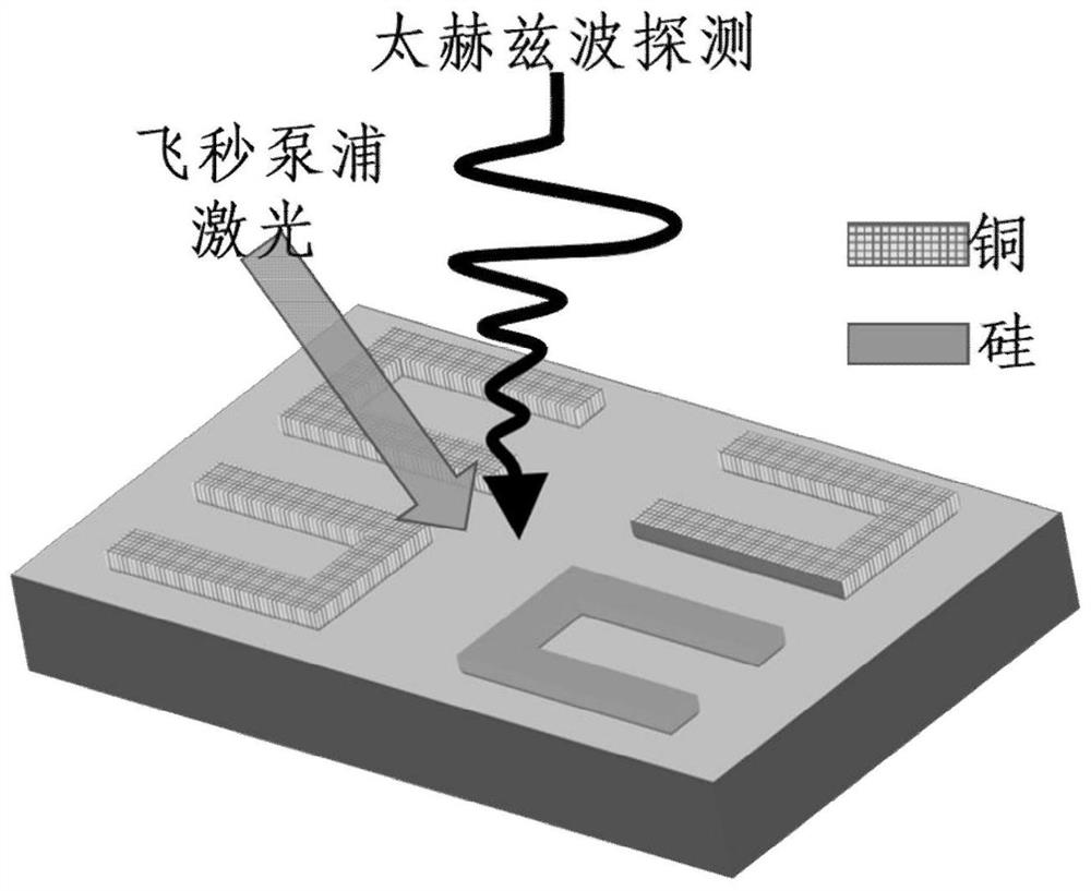
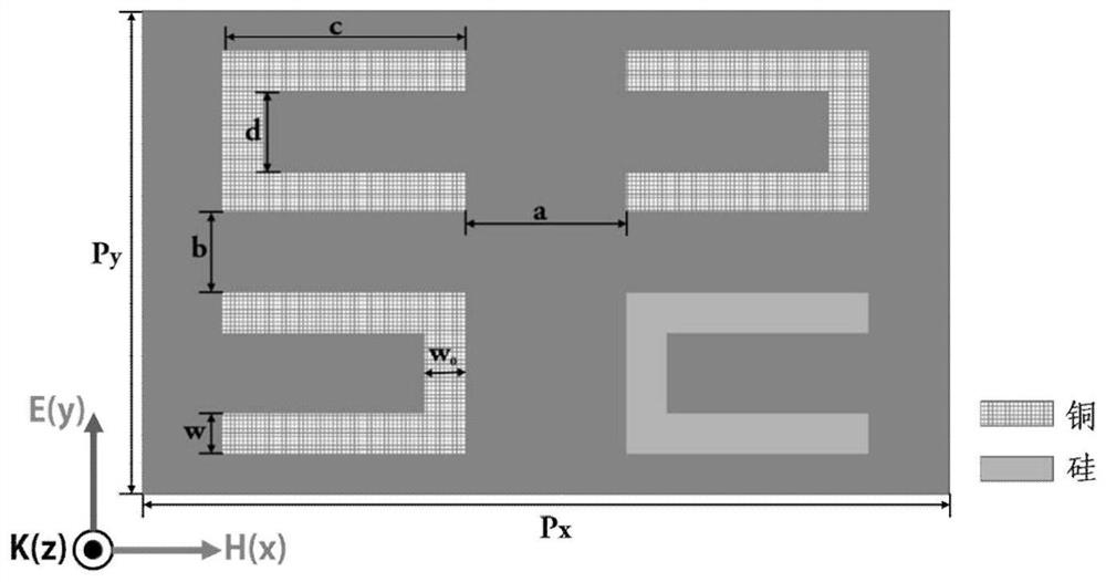
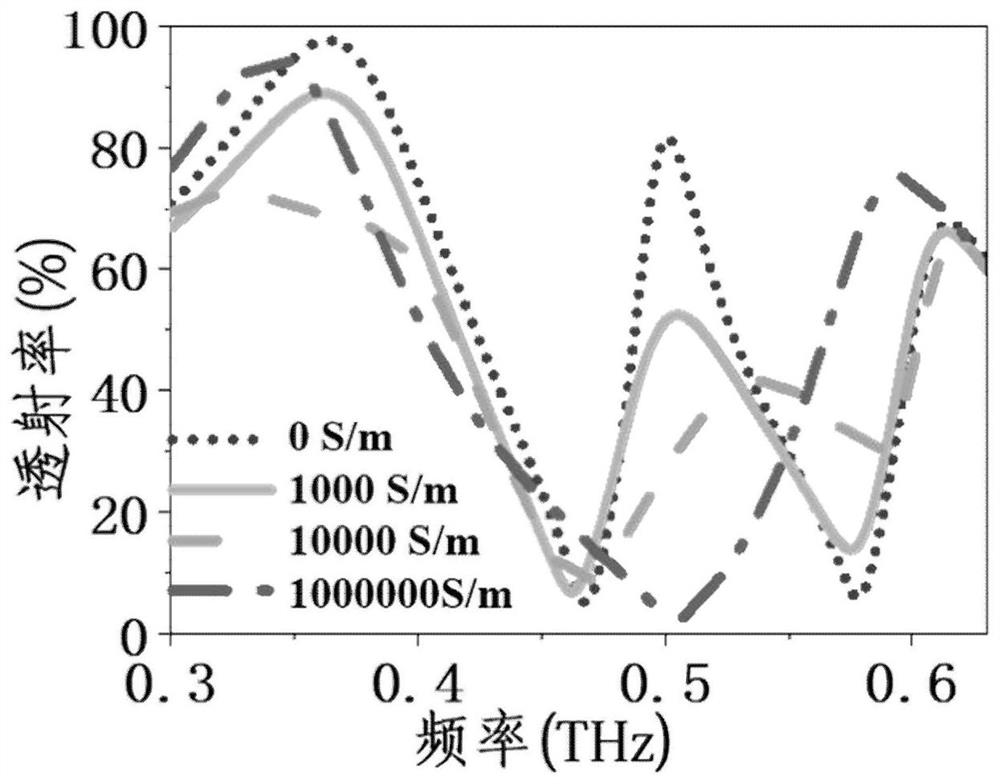
[0026] figure 1 A structural diagram of a unit array of a terahertz wave modulator based on atomic vacancy defects provided for the embodiment; figure 2 A top view structure diagram of a unit array of a terahertz wave modulator based on atomic vacancy defects provided for the embodiment. Depend on figure 1 with figure 2 It can be seen that the terahertz wave modulator of the embodiment includes a sapphire substrate with a thickness of 500 μm, and a metamaterial structure layer formed on the substrate; the metamaterial structure layer includes a plurality of metamaterial units arranged in an array, and the supermaterial structure layer The material unit is composed of four C-shaped resonant rings arranged in 2×2. The openings of the two C-shaped resonant rings in the first row are set opposite to each other, and the openings of the two C-shaped resonant rings in the second row are set in opposite directions; among them, The C-shaped resonant rings in the second row and the...


PUM

PropertyMeasurementUnit
thicknessaaaaaaaaaa
thicknessaaaaaaaaaa
thicknessaaaaaaaaaa

Abstract

The invention discloses a terahertz wave modulator based on an atomic vacancy-like defect, and belongs to the technical field of terahertz wave modulators. The modulator comprises a substrate and a metamaterial structure layer formed on the substrate, the metamaterial structure layer comprises a plurality of metamaterial units arranged in an array mode, each metamaterial unit is composed of four C-type resonance rings arranged in a 2 * 2 mode, any C-type resonance ring is made of semiconductor materials or vanadium dioxide, and the other three C-type resonance rings are made of metal materials. One C-type resonance ring in the unit structure is made of the semiconductor material or vanadium dioxide, the other three C-type resonance rings are made of the metal materials, the semiconductor material or vanadium dioxide is introduced to serve as a vacancy defect in the structural unit, and the double-resonance effect can be achieved; meanwhile, further, the active regulation and control of terahertz waves can be realized through an external excitation mode of heating or optical pumping, the structure is simple, and the stability is good.

Description

technical field [0001] The invention belongs to the technical field of terahertz wave modulators, in particular to a terahertz wave modulator based on atomic vacancy defects. Background technique [0002] Terahertz wave is an electromagnetic wave between photonics and electronics. It usually refers to electromagnetic waves in the range of 0.1THz to 10THz. It is widely used in communication, imaging, radar and other fields. At the same time, terahertz wave technology was rated as one of the "Ten Technologies that Will Change the Future World" by the United States, and was listed as the first among the "Ten Key Strategic Objectives of the National Pillar" by Japan. There is no doubt that terahertz control devices have become one of the key core devices. [0003] Metamaterials refer to artificial composite microstructure materials with electromagnetic properties that natural materials do not have. At present, there have been many studies on the use of metamaterials to regulat...

Claims


Application Information

Patent Timeline
Patent Type & Authority Applications(China)
IPC IPC(8): G02F1/015G02F1/01
CPCG02F1/015G02F1/0102
Inventor 文天龙黄洁田晨辰张怀武廖宇龙钟智勇
Owner UNIV OF ELECTRONICS SCI & TECH OF CHINA
Why Eureka
Try Eureka