

Semiconductor manufacturing method
A manufacturing method and semiconductor technology, applied in semiconductor lasers, laser parts, electrical components, etc., can solve the problems of monitoring and characterizing materials, and achieve the effect of low loss and good reliability
- Summary
- Abstract
- Description
- Claims
- Application Information
AI Technical Summary
Problems solved by technology
Method used
Image



Examples
Embodiment Construction
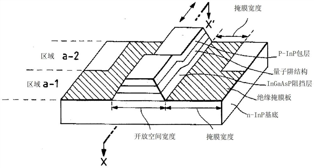
[0037]This embodiment provides a semiconductor manufacturing method for growing quantum wells with different layer thicknesses in the same plane during a single semiconductor epitaxial deposition process. First, a viaduct structure is formed on the region that needs to be modified, such as image 3 shown. The epitaxial layer under the bridge structure is thinner than the epitaxial layer outside the bridge structure due to reduced gas source diffusion under the bridge structure. Therefore, this technique results in a negative layer epitaxy rate in the modified region compared to the unmodified region, as Figure 4 As shown in (a)-(c), the inventors call this technology Selective Depletion Epitaxy SDE.
[0038] This embodiment relates to a wafer manufacturing method for growing quantum wells with different layer thicknesses in the same plane during a single semiconductor epitaxial deposition process, comprising the following steps:
[0039] Step 1, see figure 2 , implement t...
PUM
 Abstract
Description
Claims
Application Information