Photoelectric material and device impulse voltage testing device and method

A photoelectric material and impulse voltage technology, applied in the direction of measuring devices, testing dielectric strength, instruments, etc., can solve the problems of narrow carrier waveform range, large floor area, and inaccurate measurement and adjustment of voltage waveform, so as to reduce operation The effect of difficulty, low cost, fast and convenient adjustment

Pending Publication Date: 2021-06-22
成都市产品质量监督检验研究院
View PDF5 Cites 0 Cited by
  • Summary
  • Abstract
  • Description
  • Claims
  • Application Information

AI Technical Summary

Problems solved by technology

[0004] The purpose of the present invention is to provide a photoelectric material and device impulse voltage testing device in view of the above shortcomings, which solves the problems in the prior art that the impulse voltage generating device occupies a large area, has a narrow carrier waveform range, and The problem that the voltage waveform at both ends of the optoelectronic material to be tested cannot be accurately measured and adjusted

Method used


Image

  • Photoelectric material and device impulse voltage testing device and method
  • Photoelectric material and device impulse voltage testing device and method

Examples


Embodiment 1

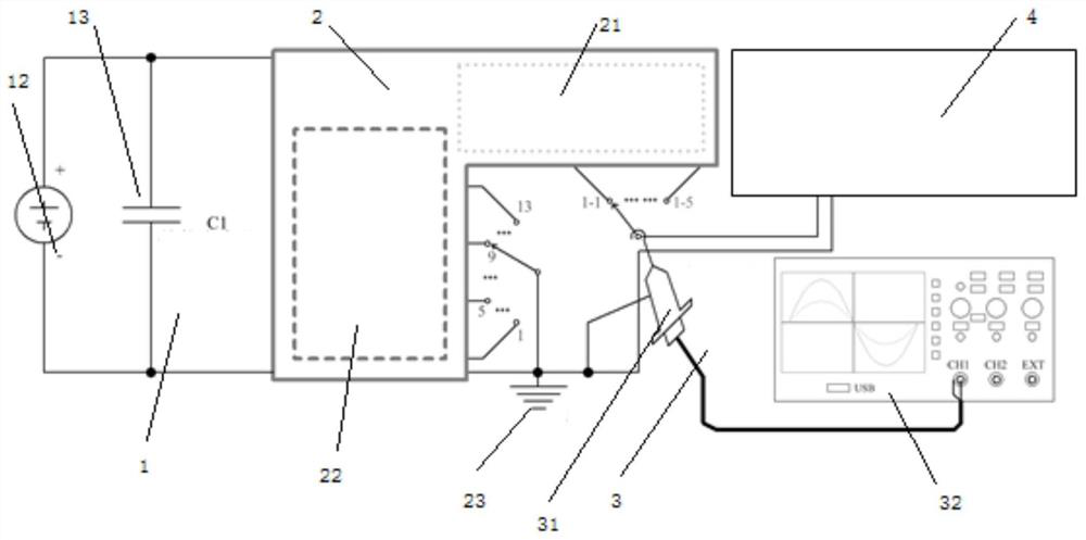
[0029] see figure 1 Or 2, the present invention provides a kind of technical scheme:

[0030] A photoelectric material and device impulse voltage testing device, comprising a charging assembly 1, an adjustment output assembly 2, a monitoring assembly 3 and a carrier to be tested 4; the charging assembly 1 is connected to the adjustment output assembly 2, and the adjustment output assembly 2 is connected to the The test carrier 4 is connected, the connection between the monitoring component 3 and the test carrier 4 , and the test component is used to monitor the voltage at both ends of the test carrier 4 .

[0031] The charging assembly 1 is used for connecting with an external power source and charging, and the charging assembly 1 includes a control panel 11, a controller, a charging power supply 12 and an energy storage capacitor 13; the charging power supply 12 is connected to the energy storage capacitor 13 , the control panel is connected to the controller, the controller...

Embodiment 2

[0043] This embodiment provides a method for testing the impulse voltage of optoelectronic materials and devices; the specific steps are as follows:

[0044] Step 1: Pressure test, according to the national standard peak voltage of different optoelectronic materials and devices, repeatedly set the capacitor reference setting voltage, and then output until the peak voltage displayed on the oscilloscope meets the national standard peak voltage;

[0045] Step 2: Wave modulation. Since the optoelectronic material and device must be impacted according to the voltage determined by the specific voltage waveform during the test to know whether the optoelectronic material and device are compliant, the output voltage waveform needs to be modulated;

[0046] First, observe the shape of the preliminary waveform in step 1, compare it with the standard waveform, control the rise time of the output waveform through the leading edge matching network 21, and reduce the resistance value in the l...

Embodiment 3

[0052] The load to be tested in this solution is a type of photovoltaic module made of 72 crystalline silicon materials. When setting the reference voltage, it needs to be gradually adjusted from low voltage to high voltage. When the voltage reaches the rated test voltage of the optoelectronic material and device, the adjustment of the voltage setting knob can be stopped, and the test of the optoelectronic material and device can be started.

[0053] When the voltage is set, turn the voltage setting knob, and the digital display voltage of the benchmark setting will change accordingly, thereby changing the output voltage of the charging power supply 12 (at this time, the charging power supply 12 has no high-voltage output, and it can only be activated after clicking the single or continuous button. output by high voltage).

[0054] When the optoelectronic material and device type are 72 crystalline silicon material photovoltaic modules and connected, and the test method is for...


PUM


Abstract

The invention discloses a photoelectric material and device impulse voltage testing device and method. The photoelectric material and device impulse voltage testing device comprises a charging assembly, an adjusting output assembly, a monitoring assembly and a to-be-tested carrier. The charging assembly is connected with the adjusting output assembly, the adjusting output assembly is connected with a to-be-detected carrier, the monitoring assembly is connected with the to-be-detected carrier, and the to-be-detected assembly is used for monitoring the voltage condition at the two ends of the to-be-detected carrier; the charging assembly is used for being connected with an external power source and conducting energy charging. The charging assembly comprises a control panel, a controller, a charging power source and an energy storage capacitor. The charging power supply is connected with the energy storage capacitor, and the control panel is connected with the controller. According to the invention, the standard waveform of the to-be-tested carrier can be rapidly obtained, adjustment can be rapidly and conveniently carried out, the impact efficiency of the photoelectric materials and devices is improved, the device can be matched with the output waveform requirements of various types of photoelectric materials and devices, adjustment is carried out according to different to-be-tested carrier materials, and the test efficiency is improved. The operation difficulty is greatly reduced, and the working efficiency is improved.

Description

technical field [0001] The invention relates to the technical field of photoelectric material and device impulse voltage testing, in particular to a photoelectric material and device impulse voltage testing device and method. Background technique [0002] The ability of optoelectronic materials and devices to resist pulse voltage is an important performance index. Impulse voltage generator (referred to as equipment, the same below) is mainly used to simulate and test the impact of lightning overvoltage, operating overvoltage and other impulse voltages on optoelectronic materials and devices to ensure their insulation and protection performance. [0003] Therefore, the test voltage is often much higher than the voltage that the equipment insulation can withstand during normal operation. Impulse voltage generator is one of the basic equipment of high voltage laboratory. With the continuous improvement of transmission voltage level and the wide application of large-capacity el...

Claims


Application Information

Patent Timeline
Patent Type & Authority Applications(China)
IPC IPC(8): G01R31/12
CPCG01R31/129
Inventor 夏庚培李添向维李建勤江瑜成皓楠任麟东
Owner 成都市产品质量监督检验研究院
Why Eureka
Try Eureka