I-shaped microstructure optical fiber electro-optical modulator based on two-dimensional material coating

A technology of microstructured optical fiber and electro-optical modulator, applied in the directions of microstructured optical fiber, cladding optical fiber, optical waveguide light guide, etc., can solve the problems of inability to meet, destroy the optical fiber structure, loss, etc., achieve low insertion loss, reduce the difficulty of realization, Effect of low modulation voltage

Inactive Publication Date: 2021-06-22
BEIJING JIAOTONG UNIV
View PDF5 Cites 1 Cited by
  • Summary
  • Abstract
  • Description
  • Claims
  • Application Information

AI Technical Summary

Problems solved by technology

However, the above-mentioned D-type optical fiber greatly destroys the original structure of the optical fiber, and the cutting surface involves the core, resulting in a huge loss, which cannot meet the needs of practical applications (about ≤1dB)

Method used


Image

  • I-shaped microstructure optical fiber electro-optical modulator based on two-dimensional material coating
  • I-shaped microstructure optical fiber electro-optical modulator based on two-dimensional material coating
  • I-shaped microstructure optical fiber electro-optical modulator based on two-dimensional material coating

Examples


Embodiment 1

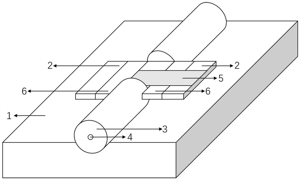
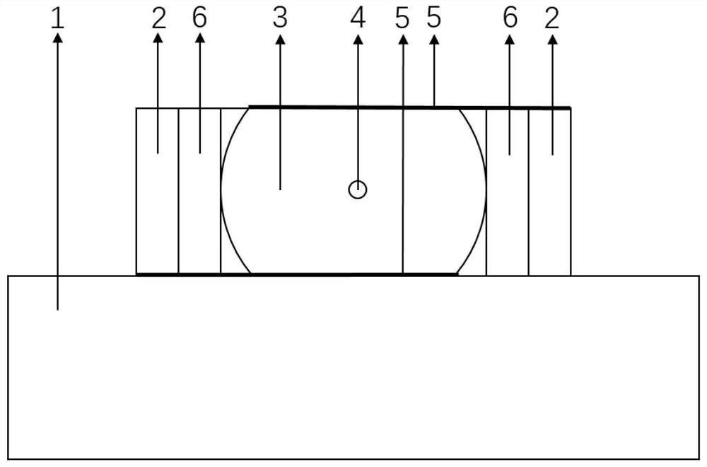
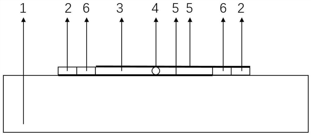
[0017] I-shaped microstructure fiber electro-optic modulator based on two-dimensional material coating such as figure 1 shown. Silicon substrate 1, electrode 2, common single-mode optical fiber cladding 3, fiber core 4, two-dimensional material film 5 and silicon support 6.

[0018] The specific combination method is as follows: the ordinary single-mode optical fiber cladding 3 is cut and ground to form an I-shaped structure, and the upper and lower layers are respectively processed to the same distance from the fiber core 4; the two-dimensional material film 5 is respectively written on the upper surface of the silicon substrate 1 and On the upper side of the I-shaped optical fiber, the I-shaped optical fiber is reversely stacked on the substrate; the electrode 2 is plated on both sides of the silicon support 6 and connected to the two-dimensional material film to provide the voltage required for modulation and change the optical signal intensity or phase.

[0019] The silic...

Embodiment 2

[0022] I-shaped microstructure fiber electro-optic modulator based on two-dimensional material coating such as figure 1 shown. Silicon substrate 1, electrode 2, common single-mode optical fiber cladding 3, fiber core 4, two-dimensional material film 5 and silicon support 6.

[0023] The specific combination method is: the ordinary single-mode optical fiber cladding 3 is cut and ground to form an I-shaped structure, and the upper and lower layers are respectively processed to the same distance from the fiber core 4 to ensure that the main part of the light field is transmitted in the fiber core; the two-dimensional material The thin film 5 is respectively written on the upper surface of the silicon substrate 1 and the upper side of the I-shaped optical fiber, and then the I-shaped optical fiber is reversely stacked on the substrate; the electrode 2 is plated on both sides of the silicon support 6 and connected with the two-dimensional material film to provide modulation. The r...

Embodiment 3

[0027] I-shaped microstructure fiber electro-optic modulator based on two-dimensional material coating such as figure 1 shown. Silicon substrate 1, electrode 2, common single-mode optical fiber cladding 3, fiber core 4, two-dimensional material film 5 and silicon support 6.

[0028]The specific combination method is as follows: the ordinary single-mode optical fiber cladding 3 is cut and ground to form an I-shaped structure, and the upper and lower layers are respectively processed to the same distance from the fiber core 4; the two-dimensional material film 5 is respectively written on the upper surface of the silicon substrate 1 and On the upper side of the I-shaped optical fiber, the I-shaped optical fiber is reversely stacked on the substrate; the electrode 2 is plated on both sides of the silicon support 6 and connected to the two-dimensional material film to provide the voltage required for modulation and change the optical signal intensity or phase.

[0029] The silico...


PUM

PropertyMeasurementUnit
widthaaaaaaaaaa
thicknessaaaaaaaaaa
thicknessaaaaaaaaaa

Abstract

The invention discloses an I-shaped microstructure optical fiber electro-optical modulator based on two-dimensional material coating. The invention belongs to the field of optical fiber devices for communication, and particularly relates to the field of optical modulation. A schematic diagram of the modulator is as shown in an abstract drawing, a common single-mode fiber cladding 3 is cut and ground to form an I-shaped structure, and the upper layer and the lower layer are respectively processed to have the same distance from a fiber core 4, so that main parts of a light field are transmitted in the fiber core; the two-dimensional material films 5 are respectively inscribed on the upper surface of the silicon substrate 1 and the upper side of the I-shaped optical fiber, and then the I-shaped optical fiber is reversely piled on the substrate; the electrodes 2 are arranged on the two sides of the silicon support 6 in a transition mode so as to provide voltage needed by modulation. Through the setting, different voltages are applied to the modulator, and the light intensity change after passing through the modulator is observed, so that parameters such as modulation depth, modulation voltage, insertion loss and the like are obtained. According to the electro-optical modulator, the insertion loss is effectively reduced through the I-shaped structure, the modulation efficiency can be improved through double-layer coating of the two-dimensional material, and the modulation voltage is reduced.

Description

technical field [0001] The invention belongs to the field of optical fiber devices for communication, in particular to the field of light modulation. Background technique [0002] In the information society, the increasing development of data communication and the Internet has prompted the market to continuously increase the demand for transmission rate and communication capacity, so that the demand for optical transmission networks has also increased rapidly. In large-capacity optical transmission systems, high-speed modulation of optical signals must be indispensable. Optical fiber communication is the cornerstone of the information industry, a research field highlighted in the "National Medium and Long-Term Development Plan", and a major issue related to the national economy, people's livelihood and national strength. Optical communication technology has made great progress in recent decades and is closely related to our lives. The design of optical devices in optical c...

Claims


Application Information

Patent Timeline
Patent Type & Authority Applications(China)
IPC IPC(8): G02F1/01G02B6/02
CPCG02B6/02295G02F1/011G02F1/0115G02F1/0118
Inventor 裴丽王吉宁提纲李晶郑晶晶阮祖亮王建帅
Owner BEIJING JIAOTONG UNIV
Why Eureka
Try Eureka