Capacitive RF MEMS switch with high reliability
A reliable and capacitive technology, applied in circuits, relays, electrical components, etc., can solve the problems of low power, low isolation, poor reliability, etc., and achieve the effect of high service life, high isolation, and high operating power
- Summary
- Abstract
- Description
- Claims
- Application Information
AI Technical Summary
Problems solved by technology
Method used
Image

Examples
Embodiment 1
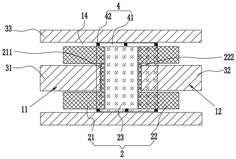
[0054] Please also refer to figure 1 and Figure 4 , the high-reliability capacitive RF MEMS switch provided by the present invention will now be described. The high-reliability capacitive RF MEMS switch includes a substrate 1, a driving part 2 arranged inside the substrate 1, a transmission part 3 and a sliding part 4 arranged on the substrate 1, and the sliding part 4 consists of The driving part 2 is driven to realize plane movement on the base 1 . Both the driving component 2 and the transmission component 3 are arranged inside the base 1 , and the driving component 2 and the transmission component 3 are located at the same height of the base 1 . Preferably, the driving component 2 and the transmission component 3 need to be arranged alternately in the horizontal layout, and the two cannot overlap each other, so as not to affect the driving or capacitive coupling.
[0055] Wherein, the two sides of the substrate 1 are respectively the input side 11 and the output side 1...
Embodiment 2
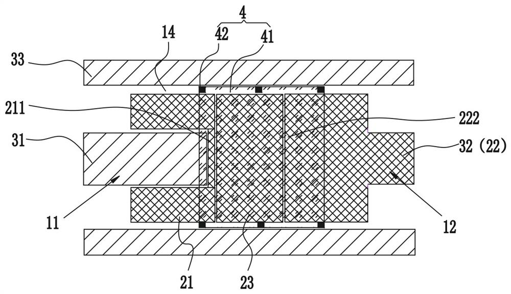
[0097] see figure 2 , as another specific implementation of the high-reliability capacitive RF MEMS switch provided by the present invention, the difference between this embodiment and Embodiment 1 is that the second driving component 22 is connected to the output part 32 , the first driving assembly 21 and the input part 31 are separated, and at this time the second driving assembly 22 and the output part 32 are the same part, which can realize simultaneous processing, the structure is simpler, and the process difficulty is lower. At the same time, the areas of the first driving component 21 and the second driving component 22 are different, the coupling capacitance is increased, the operating frequency range of the RF MEMS switch is widened, and the insertion loss is reduced.
Embodiment 3
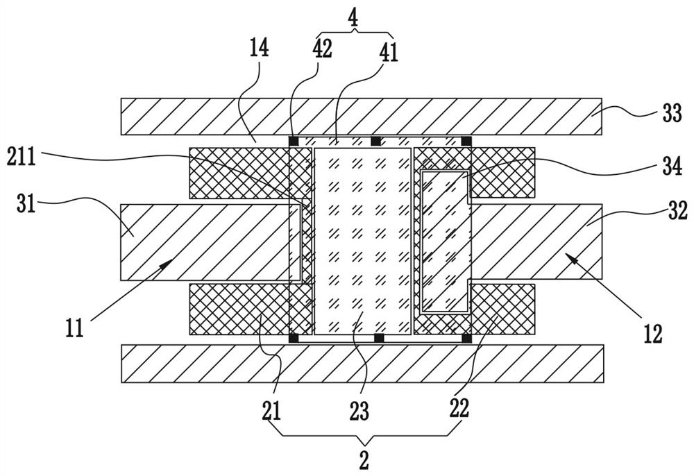
[0099] refer to image 3 , as another specific implementation of the high-reliability capacitive RF MEMS switch provided by the present invention, the difference between this embodiment and Embodiment 1 is that: the side of the output part 32 close to the input part 31 is provided with An extension part 34, the extension part 34 is in communication with the output part 32; or, the side of the input part 31 close to the output part 32 is provided with an extension part 34, and the extension part 34 is connected to the input part 31 connected. An extension part 34 is set on one side of the output part 32 or the input part 31, so that the cross-sectional areas of the input part 31 and the output part 32 are not completely equal. Part 32 forms capacitances that are not exactly the same in magnitude, which can increase transmission capacitance and reduce insertion loss.
PUM
| Property | Measurement | Unit |
|---|---|---|
| Width | aaaaa | aaaaa |
| Thickness | aaaaa | aaaaa |
| Thickness | aaaaa | aaaaa |
Abstract
Description
Claims
Application Information
 - R&D
- Intellectual Property
- Life Sciences
- Materials
- Tech Scout
- Unparalleled Data Quality
- Higher Quality Content
- 60% Fewer Hallucinations
Browse by: Latest US Patents, China's latest patents, Technical Efficacy Thesaurus, Application Domain, Technology Topic, Popular Technical Reports.
© 2025 PatSnap. All rights reserved.Legal|Privacy policy|Modern Slavery Act Transparency Statement|Sitemap|About US| Contact US: help@patsnap.com