Systems and methods for determining characteristics of semiconductor devices

A technology for semiconductors and devices, applied in the field of systems and methods for determining the characteristics of semiconductor devices, capable of solving problems such as major obstacles not being overcome

Pending Publication Date: 2021-06-29
菲拓梅里克斯公司
View PDF18 Cites 1 Cited by
  • Summary
  • Abstract
  • Description
  • Claims
  • Application Information

AI Technical Summary

Problems solved by technology

However, the teachings of these patents do not appear to overcome some of the major obstacles to the adoption of SHG as a mature technology in semiconductor manufacturing and metrology

Method used


Image

  • Systems and methods for determining characteristics of semiconductor devices
  • Systems and methods for determining characteristics of semiconductor devices
  • Systems and methods for determining characteristics of semiconductor devices

Examples


Embodiment Construction

[0237] first part

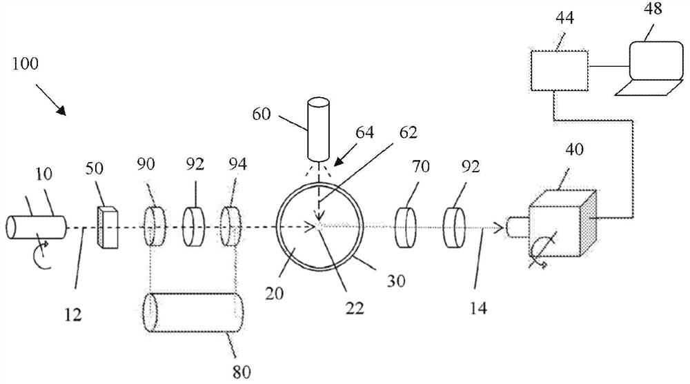
[0238] Figure 1 is a schematic diagram of a system 100 that may be used in conjunction with the methods of the present invention. For example, for intermediate optical elements, including optical delay lines and optional electrode features, in U.S. Provisional Application No. 61 / 980,860, filed April 17, 2014, entitled "WAFERMETROLOGY TECHNOLOGIES" Other suitable system variations are set forth in the section entitled "CHARGE DECAY MEASUREMENT SYSTEMS AND METHODS" referred to as Section II.

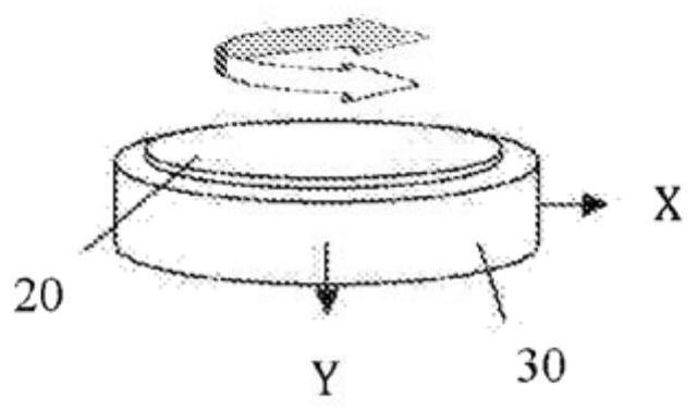
[0239] As shown, system 100 includes a primary or probe laser 10 for directing an interrogation beam 12 of electromagnetic radiation onto a sample wafer 20 held by a vacuum chuck 30 . Such as Figure 1BAs shown, the chuck 30 includes, or is disposed on, an x-stage and a y-stage, and optionally, the chuck also includes a rotary table for adjusting the position relative to the laser aiming position. Spots 22 are located on the wafer. The x-y stage enables scanning o...


PUM

PropertyMeasurementUnit
thicknessaaaaaaaaaa
thicknessaaaaaaaaaa

Abstract

Second Harmonic Generation (SHG) can be used to interrogate a surface such as a surface of a layered semiconductor structure on a semiconductor wafer. In some instances, SHG is used to evaluate an interfacial region such as between metal and oxide. Various parameters such as input polarization, output polarization, and azimuthal angle of incident beam, may affect the SHG signal. Accordingly, such parameters are varied for different types of patterns on the wafer. SHG metrology on various test structures may also assist in characterizing a sample.

Description

[0001] Cross References to Related Applications [0002] This application claims the benefit under 35 U.S.C. §119(e) of the following application, filed April 27, 2018, entitled "METHODS TO EVALUATE PATTERNED WAFER BY OPTICAL SECOND HARMONIC GENERATION" 62 / 66,942, filed April 27, 2018, entitled "PARAMETRIC MODELING FOR INTERFACIAL ELECTRIC PROPERTIES BY SHG MEASUREMENT" 62 / 663,925 of "; and "TEST STRUCTURE DESIGNFOR DETECTION OF PROCESS INDUCED CHARGING BY OPTICAL SECOND HARMONIC GENERATION (for detection of process-induced Design of Test Structures for Charging)" U.S. Provisional Application No. 62 / 663,924. technical field [0003] The present application relates to systems for Second Harmonic Generation (SHG) based wafer inspection, semiconductor metrology, material characterization, surface characterization and / or interface analysis. Background technique [0004] In nonlinear optics, the beam input is output as the sum, difference or harmonic frequencies of the inputs....

Claims


Application Information

Patent Timeline
Patent Type & Authority Applications(China)
IPC IPC(8): H01L21/66H01L27/06
CPCH01L22/30H01L22/12G01N21/9501G01N21/636G01N2021/8438G01N21/9505G01N2021/8461H01L22/34H01L27/0617G01R31/2601G01R31/2656
Inventor 雷鸣
Owner 菲拓梅里克斯公司
Why Eureka
Try Eureka