Forming method of amorphous carbon film and semiconductor structure

An amorphous carbon film and semiconductor technology, applied in semiconductor/solid-state device manufacturing, electrical components, circuits, etc., can solve the problems of low etching selection and low hardness of amorphous carbon film.

Inactive Publication Date: 2021-07-06
CHANGXIN MEMORY TECH INC
View PDF12 Cites 1 Cited by
  • Summary
  • Abstract
  • Description
  • Claims
  • Application Information

AI Technical Summary

Problems solved by technology

[0004] The present application provides a method for forming an amorphous carbon film and a semiconductor structure, which are used to solve the problems that the amorphous carbon film formed in the prior art has low hardness and relatively low etching options, so as to improve the yield of the semiconductor structure

Method used


Image

  • Forming method of amorphous carbon film and semiconductor structure
  • Forming method of amorphous carbon film and semiconductor structure
  • Forming method of amorphous carbon film and semiconductor structure

Examples


Embodiment Construction

[0034] The method for forming the amorphous carbon film and the specific implementation of the semiconductor structure provided by the present application will be described in detail below with reference to the accompanying drawings.

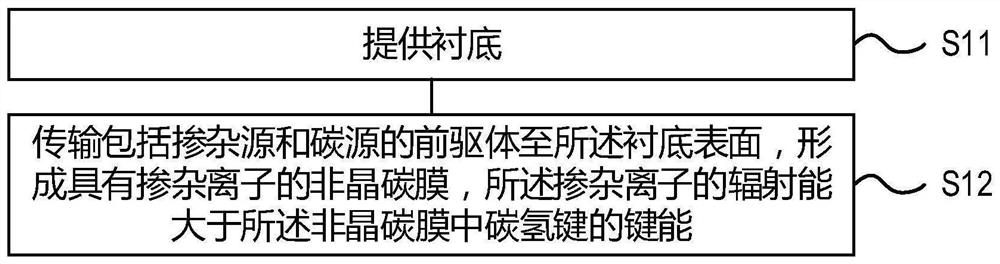
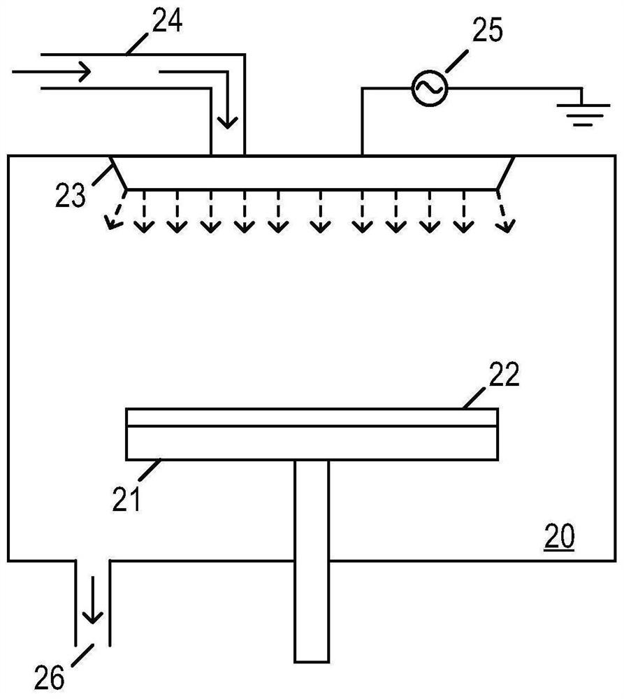
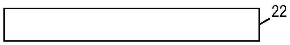
[0035] This specific embodiment provides a method for forming an amorphous carbon film, with figure 1 It is the flow chart of the formation method of the amorphous carbon film in the specific embodiment of the application, with figure 2 It is a schematic structural view of the process device used in the process of forming an amorphous carbon film in the specific embodiment of the application, with Figure 3A-3B It is a schematic cross-sectional view of the main process in the process of forming the amorphous carbon film in the specific embodiment of the present application. Such as figure 1 , figure 2 and Figure 3A-Figure 3B As shown, the method for forming the amorphous carbon film provided in this specific embodiment includes the follow...


PUM


Abstract

The invention relates to the technical field of semiconductor manufacturing, in particular to a forming method of an amorphous carbon film and a semiconductor structure. The forming method of the amorphous carbon film comprises the following steps: providing a substrate; and transmitting a precursor comprising a doping source and a carbon source to the surface of the substrate, and forming an amorphous carbon film with doped ions, wherein the radiation energy of the doped ions is larger than the bond energy of carbon-hydrogen bonds in the amorphous carbon film. According to the method, the content of the hydrogen element in the amorphous carbon film is reduced, and the carbon hydrogen ratio in the amorphous carbon film is correspondingly improved, so that the effect of improving the hardness and the etching selection ratio of the amorphous carbon film is achieved, and the method plays a positive role in improving the yield of a semiconductor structure, reducing the photoresist cost in a photoetching process and promoting the progress of a technical node.

Description

technical field [0001] The present application relates to the technical field of semiconductor manufacturing, in particular to a method for forming an amorphous carbon film and a semiconductor structure. Background technique [0002] With the shrinking of critical dimensions of integrated circuits, in order to produce high-resolution patterns, the thickness of photoresist must be reduced to increase the precision of pattern transfer. As a hard mask material with high selectivity, amorphous carbon (amorphous carbon) material is often used in pattern etching process. The amorphous carbon film is usually formed by depositing an amorphous carbon material by PECVD (Plasma Enhance Chemical Vapor Deposition, plasma enhanced chemical vapor deposition process). The use of an amorphous carbon film as a hard mask can effectively reduce the thickness of the photoresist, and when used in a pattern transfer process with a high aspect ratio, it can avoid the collapse problem caused by the...

Claims


Application Information

Patent Timeline
Patent Type & Authority Applications(China)
IPC IPC(8): H01L21/02H01L21/033
CPCH01L21/02115H01L21/02274H01L21/02318H01L21/033
Inventor 蒋昱
Owner CHANGXIN MEMORY TECH INC
Why Eureka
Try Eureka