
Composite substrate for manufacturing acoustic wave resonator, surface acoustic wave resonator and manufacturing method

A technology of acoustic resonator and composite substrate, applied in impedance network, electrical components and other directions, can solve the problems of piezoelectric sheet fragmentation, low bonding strength, piezoelectric sheet falling off, etc., to improve bonding strength and reduce acoustic wave energy loss. , the effect of preventing falling off

Pending Publication Date: 2021-07-09
NINGBO SEMICON INT CORP
View PDF19 Cites 1 Cited by
  • Summary
  • Abstract
  • Description
  • Claims
  • Application Information

AI Technical Summary

Problems solved by technology

[0006] The object of the present invention is to provide a composite substrate for making acoustic wave resonators and surface acoustic wave resonators and its manufacturing method, to solve the problem that when the piezoelectric sheet is combined with the substrate, the bonding strength is not high enough to cause the piezoelectric sheet to fall off, and the lateral direction of the piezoelectric sheet Fragmentation of piezoelectric sheets caused by deformation

Method used


Image

  • Composite substrate for manufacturing acoustic wave resonator, surface acoustic wave resonator and manufacturing method
  • Composite substrate for manufacturing acoustic wave resonator, surface acoustic wave resonator and manufacturing method
  • Composite substrate for manufacturing acoustic wave resonator, surface acoustic wave resonator and manufacturing method

Examples


no. 1 example

[0040] Please refer below Figure 2 to Figure 8 A method for manufacturing the composite substrate will be described. Figure 2 to Figure 8It is a structural schematic diagram corresponding to each step in the first embodiment of the manufacturing method of the composite substrate of the present invention.

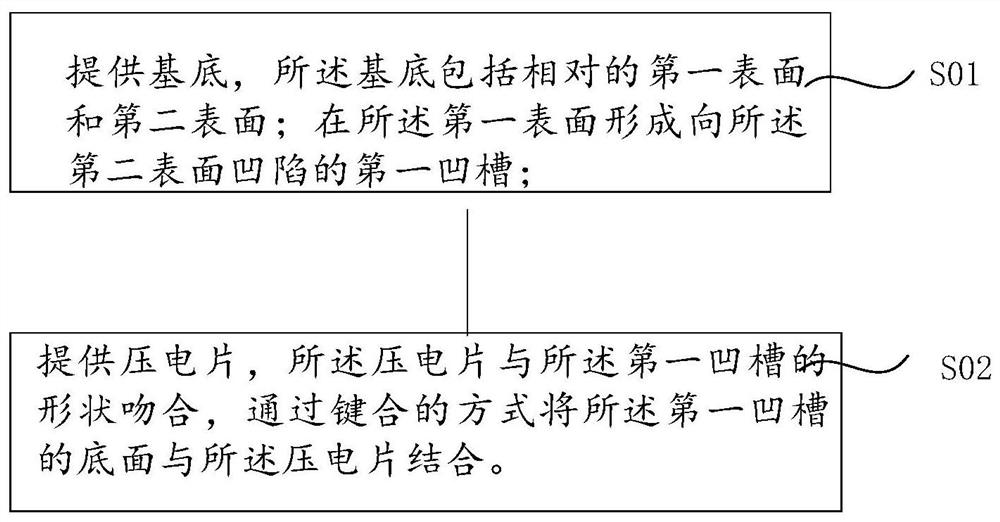
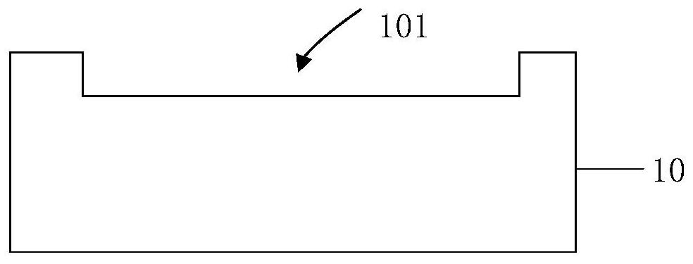
[0041] refer to figure 2 and image 3 Step S01 is performed to provide a substrate 10, the substrate 10 includes a first surface and a second surface opposite to each other, and a first groove 101 recessed toward the second surface is formed on the first surface.

[0042] The substrate 10 is used as the carrier of the piezoelectric sheet, has a low coefficient of thermal expansion, and is suitable for semiconductor processing technology. In this embodiment, the substrate is an 8-inch silicon wafer with a thickness of about 600-800 microns. In other embodiments, the substrate 10 can also be any one of the following materials: sapphire, crystal, germanium (Ge), silicon ...

no. 2 example

[0077] The difference between this embodiment and the previous embodiment is: a protrusion is formed on the bottom surface of the first groove, and a second groove is formed on the bottom surface of the piezoelectric sheet; or, a second groove is formed on the bottom surface of the first groove. a groove, forming a protrusion on the bottom surface of the piezoelectric sheet;

[0078] The protrusion matches the shape of the second groove and is located in the non-device area of ​​the composite substrate. When the piezoelectric sheet is embedded in the first groove, the second groove and the protrusion engage together.

[0079] Specifically, refer to Figure 9A to Figure 12 , before forming the first bonding layer 13, further comprising:

[0080] A plurality of protrusions 30 are formed on the bottom surface of the first groove 101; the height of the protrusions 30 may be lower than the first surface, or higher than the first surface. refer to Figure 9A , the height of the ...

no. 3 example

[0096] The third embodiment of the present invention also provides a composite substrate, Figure 8 It is a structural schematic diagram of a composite substrate according to an embodiment of the present invention, please refer to Figure 8 , the composite substrate includes:

[0097] a substrate 10 comprising opposing first and second surfaces;

[0098] The first surface is provided with a first groove recessed toward the second surface;

[0099] A piezoelectric sheet 20, the piezoelectric sheet 20 is embedded in the first groove and bonded to the substrate 10, the top surface of the piezoelectric sheet 20 is higher than the first surface or is combined with the The surface of the substrate is flat. In this implementation, the surface of the composite substrate is plane. The bonding method includes one of covalent bonding, adhesive bonding and fusion bonding. For a description of the specific bonding method, please refer to the relevant content in the Methods section.

...


PUM

PropertyMeasurementUnit
Thicknessaaaaaaaaaa
Thicknessaaaaaaaaaa
Thicknessaaaaaaaaaa

Abstract

The invention discloses a composite substrate for manufacturing an acoustic wave resonator, a surface acoustic wave resonator and a manufacturing method, and the manufacturing method of the composite substrate comprises the steps: providing a substrate which comprises a first surface and a second surface which are opposite to each other; forming a first groove which is recessed towards the second surface on the first surface; and providing a piezoelectric plate, wherein the piezoelectric plate is matched with the first groove in shape, and the bottom face of the first groove is combined with the piezoelectric plate in a bonding mode. The composite substrate comprises a substrate, wherein the first substrate comprises a first surface and a second surface which are opposite; the first surface is provided with a first groove which is recessed towards the second surface; a piezoelectric plate is embedded in the first groove, and the top surface of the piezoelectric plate is higher than the first surface or is flush with the first surface.

Description

technical field [0001] The invention relates to the field of semiconductor manufacturing, in particular to a compound substrate for making an acoustic wave resonator and a surface acoustic wave resonator and a manufacturing method. Background technique [0002] With the development of mobile communication technology, the amount of mobile data transmission is also increasing rapidly. Therefore, under the premise of limited frequency resources and the use of as few mobile communication devices as possible, improving the transmission power of wireless power transmission equipment such as wireless base stations, micro base stations or repeaters has become a problem that must be considered, and it also means that the The requirements for filter power in the front-end circuit of mobile communication equipment are also getting higher and higher. Lithium tantalate or lithium niobate is widely used as a piezoelectric material for surface acoustic wave (SAW) devices. [0003] Surfac...

Claims


Application Information

Patent Timeline
IPC IPC(8): H03H9/17H03H3/02
CPCH03H9/17H03H3/02H03H9/02574H03H9/02559H03H3/08H03H9/25
Inventor 黄河罗海龙李伟齐飞
Owner NINGBO SEMICON INT CORP
Learn More