

Photo-thermal deflection spectrum testing device with wide wavelength coverage
A photothermal deflection and spectral testing technology, which is applied in the field of spectral detection, can solve the problems that low power output test devices and photothermal deflection spectral test devices cannot meet the high sensitivity test requirements of narrow bandgap materials and wide bandgap materials, and achieve high detection Sensitivity, easy installation and operation, and simple structure of the device
- Summary
- Abstract
- Description
- Claims
- Application Information
AI Technical Summary
Problems solved by technology
Method used
Image

Examples
Embodiment Construction
[0033] The present invention will be further described in detail below with reference to the accompanying drawings and embodiments. It should be noted that the following embodiments are intended to facilitate the understanding of the present invention, but do not limit it in any way.
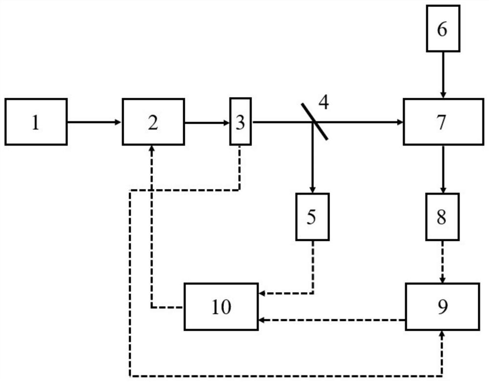
[0034] Such as figure 1 As shown, a photothermal deflection spectroscopy test device with wide wavelength coverage, including a pump light source 1, a monochromator 2, an optical chopper 3, a beam splitter 4, a detection light source 6, an absorption cell 7, and a position-sensitive detector 8. Devices such as photodetector 5, lock-in amplifier 9 and computer 10. The entire photothermal deflection spectroscopy test device is built on a shock-isolation platform.
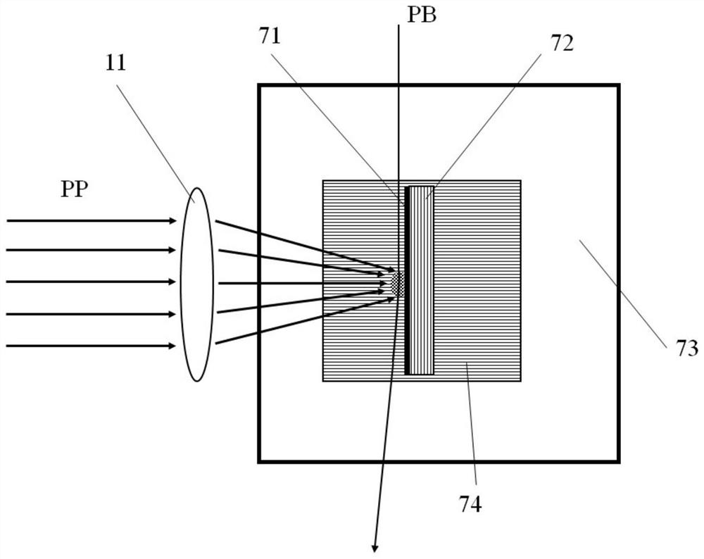
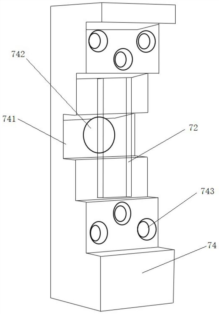
[0035] Among them, the pumping light source 1, the monochromator 2, the optical chopper 3 and the beam splitter 4 are sequentially arranged along the optical path; An absorption pool 7 is arranged; the signal output end of the photode...
PUM
| Property | Measurement | Unit |
|---|---|---|
| diameter | aaaaa | aaaaa |
Abstract
Description
Claims
Application Information