Transient voltage suppression device and manufacturing method thereof

An instantaneous voltage and device technology, which is applied in the field of instantaneous voltage suppression devices and its manufacturing, can solve the problems of large chip size, unfavorable device miniaturization, large resistance, etc., and achieve the effect of reducing the clamping voltage and reducing the size

Active Publication Date: 2021-07-16
HANGZHOU SILAN INTEGRATED CIRCUIT
View PDF10 Cites 3 Cited by
  • Summary
  • Abstract
  • Description
  • Claims
  • Application Information

AI Technical Summary

Problems solved by technology

[0006] Although the existing TVS devices can provide low breakdown voltage and low capacitance to meet the requirements of low voltage and high speed, due to the configuration of the I / O port protection diode, when the voltage of the I / O port is higher than the Zener diode breakdown voltage When , the current flows out through the PIN diode, n+ buried layer and clamp diode to the substrate
Due to the long current path and the limitation of the integrated circuit process, the resistance of the n+ buried layer is relatively large. To achieve a larger peak-to-peak current Ipp and a smaller clamping voltage in the breakdown direction, a larger chip size is required. It is not conducive to the miniaturization of the device

Method used


Image

  • Transient voltage suppression device and manufacturing method thereof
  • Transient voltage suppression device and manufacturing method thereof
  • Transient voltage suppression device and manufacturing method thereof

Examples


Embodiment Construction

[0086] Various embodiments of the invention will be described in more detail below with reference to the accompanying drawings. In the various drawings, the same elements are denoted by the same or similar reference numerals. For the sake of clarity, various parts in the drawings have not been drawn to scale.

[0087] The specific implementation manners of the present invention will be further described in detail below in conjunction with the accompanying drawings and embodiments.

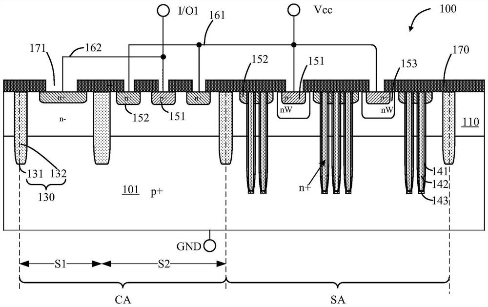
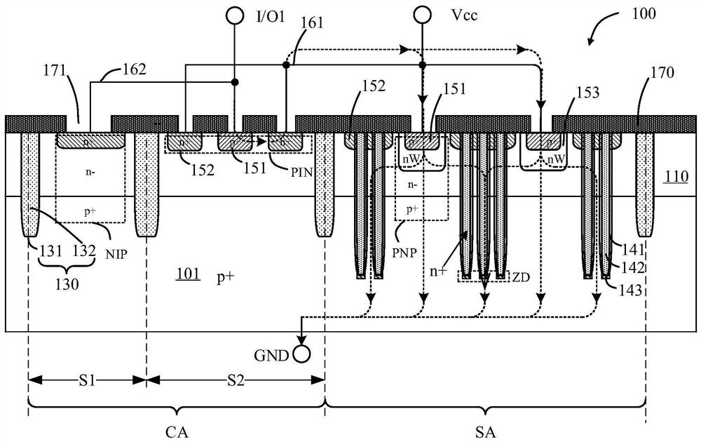
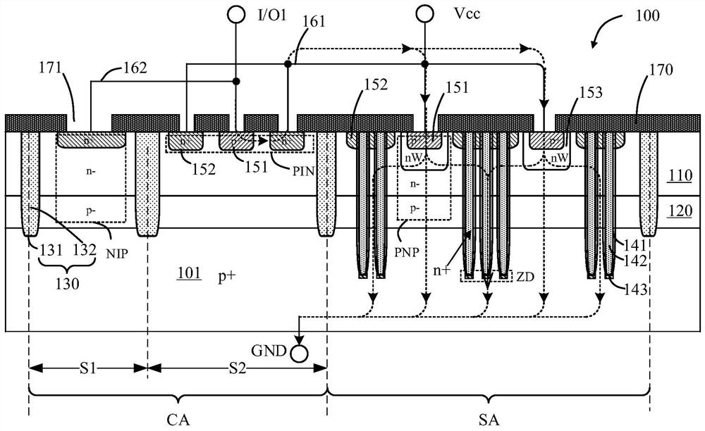
[0088] Figure 1a and Figure 1b A schematic cross-sectional view and a schematic current path of the transient voltage suppression device provided by the first embodiment of the present invention are shown respectively. like Figure 1a As shown, the transient voltage suppression device 100 includes a semiconductor substrate 101, a first epitaxial layer 110 located on the semiconductor substrate 101, a plurality of isolation structures 130, a plurality of first trench structures, a first implanta...


PUM

PropertyMeasurementUnit
depthaaaaaaaaaa
depthaaaaaaaaaa
electrical resistivityaaaaaaaaaa

Abstract

The invention discloses a transient voltage suppression device and a manufacturing method thereof. The transient voltage suppression device comprises a semiconductor substrate, a first epitaxial layer located on the semiconductor substrate, a plurality of isolation structures, a plurality of first groove structures, a first injection region and a second injection region; the isolation structures penetrate through the first epitaxial layer and extend into the semiconductor substrate, the plurality of isolation structures divide the transient voltage suppressor into a plurality of regions in the transverse direction, the plurality of regions comprise a voltage stabilization region and at least one group of guide diode regions, and each group of guide diode regions comprise a first region and a second region; the plurality of first groove structures are positioned in the voltage stabilization region and penetrate through the first epitaxial layer; the first injection region is located in the first epitaxial layer of the second region and the voltage stabilization region; and the second injection region is located in the first epitaxial layer of the first region and the second region. A clamping diode and a triode are formed in the voltage stabilization region, the clamping diode and the triode form a composite voltage stabilizing tube, the clamping diode and the triode share current at the same time, the peak-peak value current in the breakdown direction is improved, the clamping voltage during large current conduction is reduced, and the size of the device is reduced.

Description

technical field [0001] The invention relates to the technical field of semiconductor manufacturing, in particular to a transient voltage suppression device and a manufacturing method thereof. Background technique [0002] With the continuous development of integrated circuit technology, the volume of devices becomes smaller and the operating voltage becomes lower and lower. At the same time, devices are getting faster and operating at higher frequencies. Therefore, it is more difficult to implement a transient voltage suppressor (TVS) or electrostatic discharge (ESD) protection device to meet the needs of today's integrated circuits. TVS or ESD devices must provide low breakdown voltage and low capacitance to meet the requirements of low voltage and high speed, and also need to meet the smallest possible chip size, larger peak-peak current Ipp in the breakdown direction and smaller clamp bit voltage requirements. [0003] Some conventional TVS or ESD protection devices us...

Claims


Application Information

Patent Timeline
Patent Type & Authority Applications(China)
IPC IPC(8): H01L27/02
CPCH01L27/0292H01L27/0259H01L27/0255
Inventor 王英杰
Owner HANGZHOU SILAN INTEGRATED CIRCUIT
Why Eureka
Try Eureka