A semiconductor device with high robustness and its manufacturing method

A semiconductor and robust technology, applied in the field of semiconductor devices with high robustness, can solve the problems of increased electric field strength, increased device resistance, increased device cost, etc., to reduce peak voltage, improve current change rate, and improve endurance The effect of pressure

Active Publication Date: 2022-06-24
上海擎茂微电子科技有限公司
View PDF7 Cites 0 Cited by
  • Summary
  • Abstract
  • Description
  • Claims
  • Application Information

AI Technical Summary

Problems solved by technology

In the process of semiconductor design and manufacturing, the performance requirements of the device and the robustness of the performance are a pair of contradictions to a certain extent. Often the better the performance of the device, the worse its robustness. In order to balance good performance and strong robustness Robustness, some manufacturers solve the problem of device performance and robustness by adding a layer of photolithography and other processes, but this increases the cost of device production
In addition, in order to improve the robustness of the device, some manufacturers have increased the size of the semiconductor device. In the planar gate bipolar transistor, on the one hand, the size of the polysilicon cannot be increased casually due to the restriction of the breakdown voltage, and the size increases to a certain extent. The electric field strength under the polysilicon will increase sharply, causing the breakdown voltage to fail. On the other hand, the size of the polysilicon cannot be reduced casually. If the size of the polysilicon is reduced to a certain extent, the carrier concentration on the upper surface of the device will be very small, thus When the device is turned on, the resistance increases, the voltage drop increases, and the loss when it is turned on increases. Under the certain size limit of the polysilicon, the distance between the polysilicons cannot be changed.
[0003] For this reason, an N+ plate is added in the traditional device design process, and arsenic is selectively injected as the source of electrons, electrons are introduced when it is turned on, and holes are drawn out when it is turned off, but this method also increases the device production. the cost of

Method used


Image

  • A semiconductor device with high robustness and its manufacturing method
  • A semiconductor device with high robustness and its manufacturing method

Examples


Embodiment Construction

[0023] The specific embodiments of the present invention will be described in further detail below with reference to the accompanying drawings and embodiments. The following examples are intended to illustrate the present invention, but not to limit the scope of the present invention.

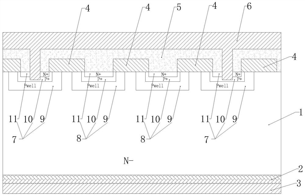
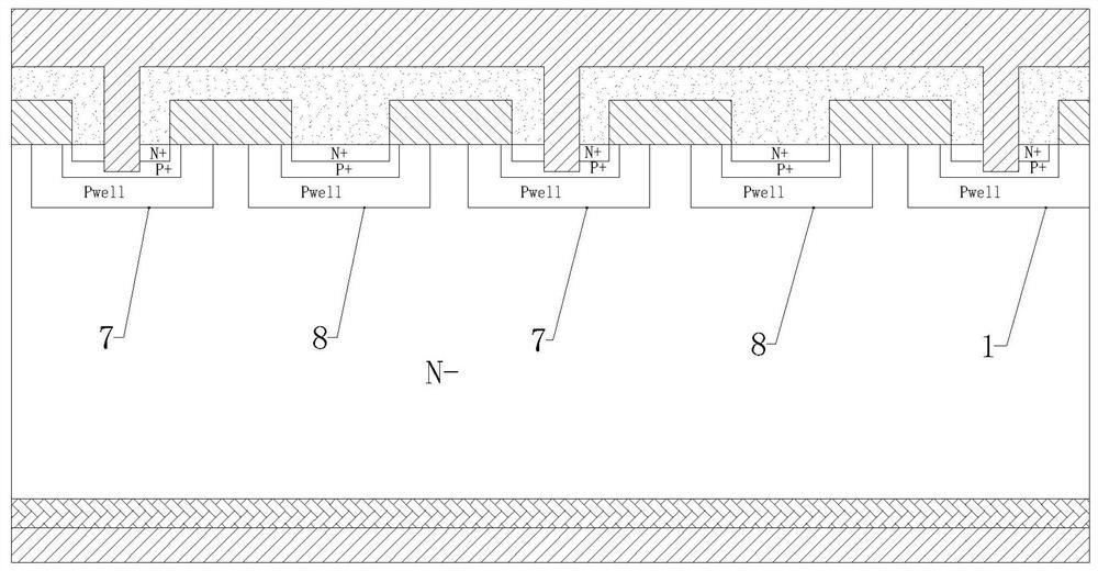
[0024] see Figure 1 to Figure 2 , a semiconductor device with high robustness according to a preferred embodiment of the present invention includes a semiconductor substrate 1, a collector electrode 2 and a collector metal layer 3 arranged on the back of the semiconductor substrate, and a gate oxide layer arranged on the surface of the semiconductor substrate and a plurality of gate polysilicon 4 above the gate oxide layer, an insulating dielectric layer 5 and a metal interconnection layer 6 located above the gate polysilicon, and a plurality of effective source regions 7 and vertical carrier adjustment regions are also provided on the surface of the semiconductor substrate 8. The effective s...


PUM

PropertyMeasurementUnit
thicknessaaaaaaaaaa
thicknessaaaaaaaaaa
thicknessaaaaaaaaaa

Abstract

The invention relates to a semiconductor device with high robustness, comprising a semiconductor substrate, a collector electrode and a metal layer of the collector electrode arranged on the back of the semiconductor substrate, a gate oxide layer arranged on the surface of the semiconductor substrate, and multiple layers above the gate oxide layer. a gate polysilicon, an insulating dielectric layer and a metal interconnection layer located above the gate polysilicon, and is characterized in that: the surface of the semiconductor substrate is also provided with a plurality of effective source regions and vertical carrier adjustment regions, the effective source regions or vertical carrier adjustment regions. The carrier adjustment region is located between the adjacent gate polysilicon, the effective source region and the vertical carrier adjustment region both include a well region, a first carrier doped region above the well region, and a first carrier doped region located in the first carrier doped region. In the upper second carrier-doped region, the effective source region is electrically connected to the metal interconnection layer, and the vertical carrier adjustment region is electrically isolated from the metal interconnection layer. The robust semiconductor device of the present invention is small in size and low in cost. In addition, the present invention also provides a method of manufacturing the semiconductor device.

Description

technical field [0001] The present invention relates to a semiconductor device, in particular to a semiconductor device with high robustness, and furthermore, the present invention also relates to a preparation method of the semiconductor device. Background technique [0002] With the gradual improvement of the requirements for the electrical characteristics of power devices, their power is getting larger and larger, and the robustness requirements of power devices are also getting higher and higher, which is mainly reflected in that the short-circuit peak current of the device needs to be kept in the safe working area as much as possible. inside. In the process of semiconductor design and manufacture, the performance requirements of the device and the robustness of the performance are a pair of contradictions to a certain extent. Often the better the performance of the device, the worse the robustness. In order to take into account good performance and strong robustness Ro...

Claims


Application Information

Patent Timeline
Patent Type & Authority Patents(China)
IPC IPC(8): H01L29/06H01L21/331H01L29/739
CPCH01L29/0611H01L29/0692H01L29/7395H01L29/66333
Inventor 王海军
Owner 上海擎茂微电子科技有限公司
Why Eureka
Try Eureka