Thin-film solar cell structure based on different scribe lines and preparation method thereof
A solar cell and thin film technology, applied in circuits, photovoltaic power generation, electrical components, etc., can solve problems such as poor conductivity, ineffective contact between grid lines and back electrode layers, and serious battery thermal effects, achieving strong practicability and avoiding problems. Battery thermal effect problem, the effect of reducing series resistance
- Summary
- Abstract
- Description
- Claims
- Application Information
AI Technical Summary
Problems solved by technology
Method used
Image
Examples
Embodiment 1
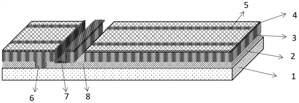
[0053] see figure 1 , a thin-film solar cell structure based on different scribing lines, which sequentially includes a substrate 1, a bottom electrode 2, a PN junction film layer 3, and a TCO layer 4 from bottom to top;
[0054] The bottom electrode 2 is provided with a P1 scribe groove 6, and the P1 scribe groove 6 extends to the upper surface of the substrate 1; the TCO layer 4 is provided with a P2 scribe groove 7 and a P3 scribe groove 8, and the bottom of the P2 scribe groove 7 The bottom of the groove 8 and P3 extend to the upper surface of the bottom electrode 2; the upper surface of the TCO layer 4 is provided with grid lines 5; the groove 6 of P1 is filled with the film layer 3 of the PN junction region; 7 is filled with conductive material.
Embodiment 2
[0056] Except for the following content, all the other contents are the same as in Example 1.
[0057] There are several grooves 6 in P1;
[0058] The size range of the P1 line groove 6 is 1 μm in line width, and the distance between the centers of adjacent P1 line grooves 6 is 3 mm.
[0059] The size range of the P2 reticle groove 7 is 10 μm in line width, and the distance between the center of the P2 reticle groove 7 and the center of the P1 reticle groove 6 is 30 μm;
[0060] The size range of the P3 scribed groove 8 is 10 μm in line width, and the distance between the center of the P3 scribed groove 8 and the center of the P2 scribed groove 7 is 30 μm.
[0061] The size range of the grid lines 5 is 5 μm in line width, and the distance between the centers of two adjacent grid lines 5 is 300 μm. The filling thickness of the conductive material was 100 μm.
Embodiment 3
[0063] Except for the following content, all the other contents are the same as in Example 1.
[0064] The size range of the P1 scoring groove 6 is 100 μm in line width, and the distance between the centers of adjacent P1 scoring grooves 6 is 30 mm.
[0065] The size range of the P2 reticle groove 7 is 100 μm in line width, and the distance between the center of the P2 reticle groove 7 and the center of the P1 reticle groove 6 is 300 μm;
[0066] The size range of the P3 line groove 8 is 100 μm in line width, and the distance between the center of the P3 line groove 8 and the center of the P2 line groove 7 is 300 μm.
[0067] The size range of the grid lines 5 is 50 μm in line width, and the distance between the centers of two adjacent grid lines 5 is 5000 μm. The filling thickness of the conductive material was 100 μm.
PUM
| Property | Measurement | Unit |
|---|---|---|
| thickness | aaaaa | aaaaa |
| thickness | aaaaa | aaaaa |
| thickness | aaaaa | aaaaa |
Abstract
Description
Claims
Application Information


