circuit board

A technology of circuit board and circuit layout, applied in the direction of circuit, printed circuit, printed circuit, etc., can solve problems such as bump bridge short circuit

Active Publication Date: 2022-02-11
CHIPBOND TECH
View PDF9 Cites 0 Cited by
  • Summary
  • Abstract
  • Description
  • Claims
  • Application Information

AI Technical Summary

Problems solved by technology

[0002] see figure 1 , the existing flip-chip packaging technology is to thermally compress a plurality of bumps 21 of a chip (not shown) to a plurality of inner pins 12 in the chip setting area 11 of the substrate 10 in a thermocompression bonding process, However, as the electrical function of the chip increases, the number of bumps 21 of the chip for electrically connecting the inner pins 12 also increases, reducing or not changing the area of ​​the chip setting area. Under certain conditions, adjacent bumps are prone to bridging short circuits

Method used


Image

  • circuit board
  • circuit board
  • circuit board

Examples


no. 1 example

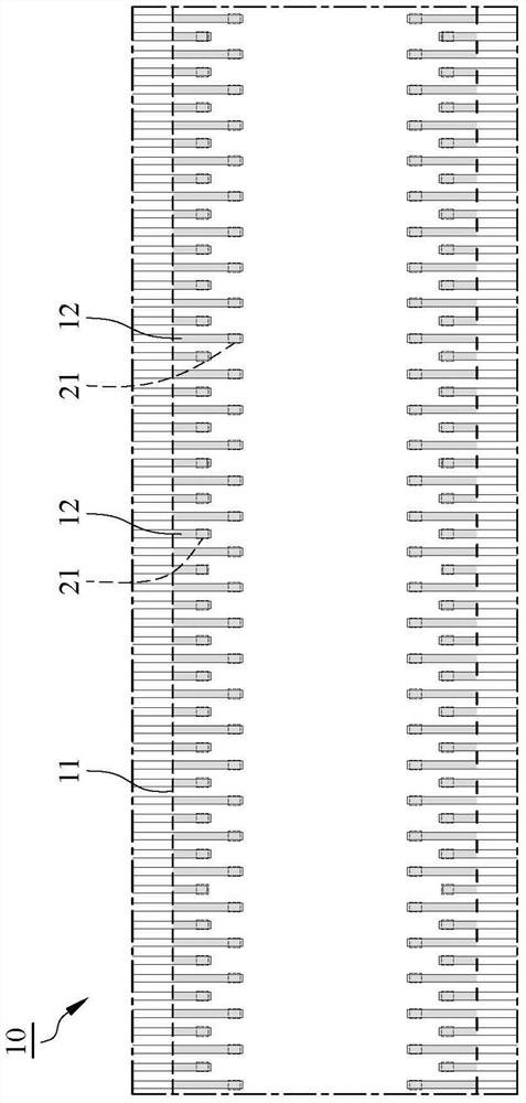
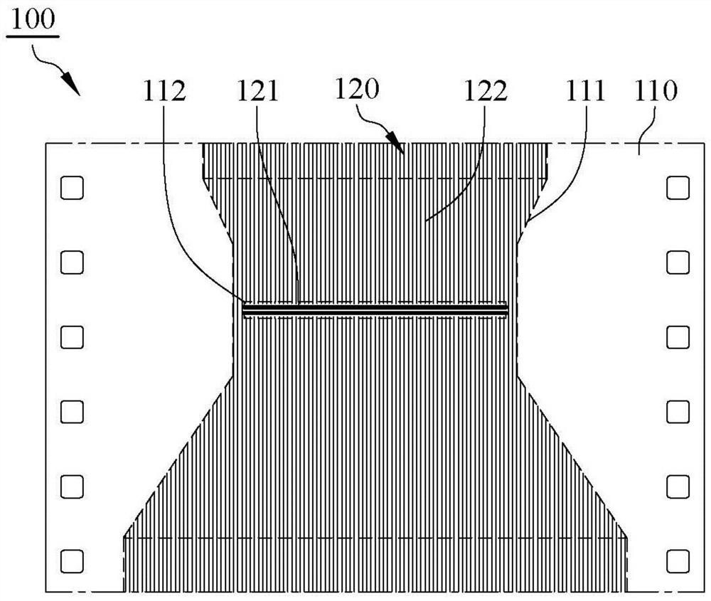
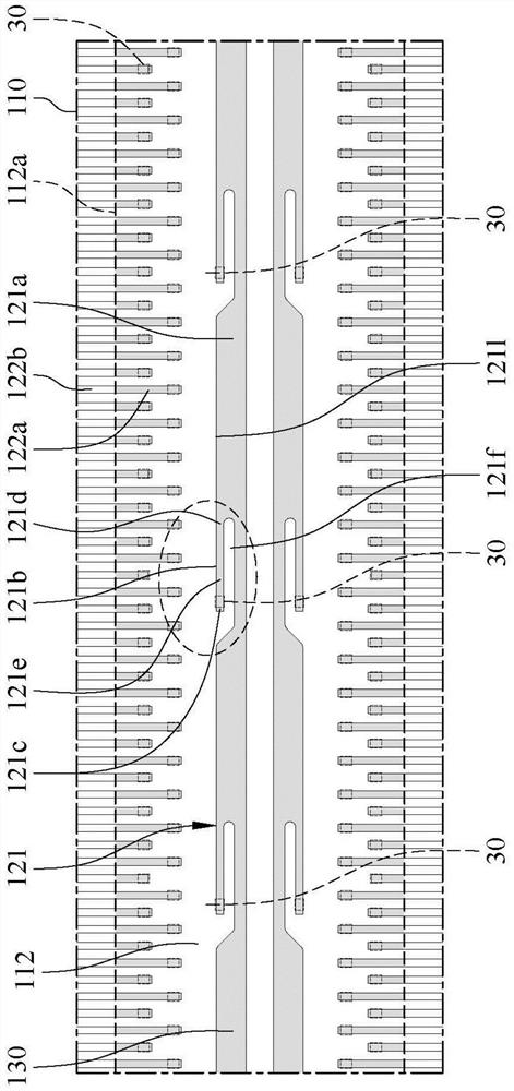
[0043] see figure 2 , image 3 and Figure 4 , the first embodiment of a circuit board 100 of the present invention, the circuit board 100 includes a substrate 110 and a circuit layer 120, preferably, the circuit board 100 further includes a solder layer 130, the solder layer 130 covers the circuit layer 120 , and the thickness of the solder layer 130 is not more than 0.3 μm, please refer to figure 2 , the substrate 110 has a circuit layout area 111 and a chip setting area 112, the chip setting area 112 is used for setting chips (not shown in the figure), and the chip setting area 112 is the bump setting area of ​​the chip projected onto the substrate 110 The bump setting area is provided with a plurality of bumps 30 .

[0044] see figure 2 , image 3 and Figure 4 , the circuit layer 120 has at least one first circuit 121 and a plurality of second circuits 122, each of the second circuits 122 includes an inner pin 122a and a base line 122b, the base line 122b is conn...


PUM


Abstract

The invention discloses a circuit board for electrically connecting chips. The circuit board includes a substrate and a circuit layer. The circuit layer has at least one first circuit and a plurality of second circuits, and the plurality of second circuits are arranged on the circuit layer. In the circuit layout area of ​​the substrate, the first line is arranged in the chip installation area of ​​the substrate, the first line includes a main line and at least one branch pin, the branch pin is connected to the main line by a connecting segment, and the branch pin There is a gap between the extension section and the bonding section to the main circuit, the bonding section is used to bond the bump of the chip, and the lead pin of the circuit board bonding the chip is increased by the tributary pin, and because the bonding section , There is a gap between the extension section and the main circuit, so in the thermocompression process, the solder disposed on the main circuit can be prevented from flowing along the branch pin to the direction of the bump, and then the tributary pin solder overflows out of the tributary pin.

Description

technical field [0001] The present invention relates to a circuit board, especially a circuit board (such as a flexible circuit board, etc.) provided with a main circuit and at least one branch pin in a chip setting area. Background technique [0002] see figure 1 , in the existing flip chip packaging technology, in the thermocompression bonding process, a plurality of bumps 21 of a chip (not shown in the figure) are thermocompressed to a plurality of inner pins 12 in the chip setting area 11 of the substrate 10, However, as the electrical functions of the chip increase, the number of the bumps 21 of the chip for electrically connecting the inner pins 12 also increases, reducing or not changing the area of ​​the chip setting area. Under the condition of , adjacent bumps are prone to bridge short circuit. SUMMARY OF THE INVENTION [0003] The main purpose of the present invention is to set a plurality of inner pins, a main circuit and at least one branch pin in the chip s...

Claims


Application Information

Patent Timeline
Patent Type & Authority Patents(China)
IPC IPC(8): H05K1/02H05K1/11H05K1/18
CPCH05K1/02H05K1/11H05K1/118H05K1/18H05K1/0393H05K1/111H05K1/189H05K2201/09227H05K2201/09236H05K2201/09254H05K2201/0969H05K3/3442H05K2201/09445Y02P70/50H05K1/115H05K1/181H01L23/12
Inventor 马宇珍黄信豪周文复许国贤
Owner CHIPBOND TECH
Why Eureka
Try Eureka