
LED epitaxial structure and growth method thereof

A growth method and epitaxial structure technology are applied in the field of LED manufacturing to achieve the effects of improving efficiency, improving luminous efficiency and expanding capacitance

Active Publication Date: 2021-07-23
XIANGNENG HUALEI OPTOELECTRONICS
View PDF9 Cites 0 Cited by
  • Summary
  • Abstract
  • Description
  • Claims
  • Application Information

AI Technical Summary

Problems solved by technology

[0004] The object of the present invention is to provide an LED epitaxial structure and its growth method to solve the problem of improving the luminous brightness of LED devices

Method used


Image

  • LED epitaxial structure and growth method thereof
  • LED epitaxial structure and growth method thereof

Examples


Embodiment 1

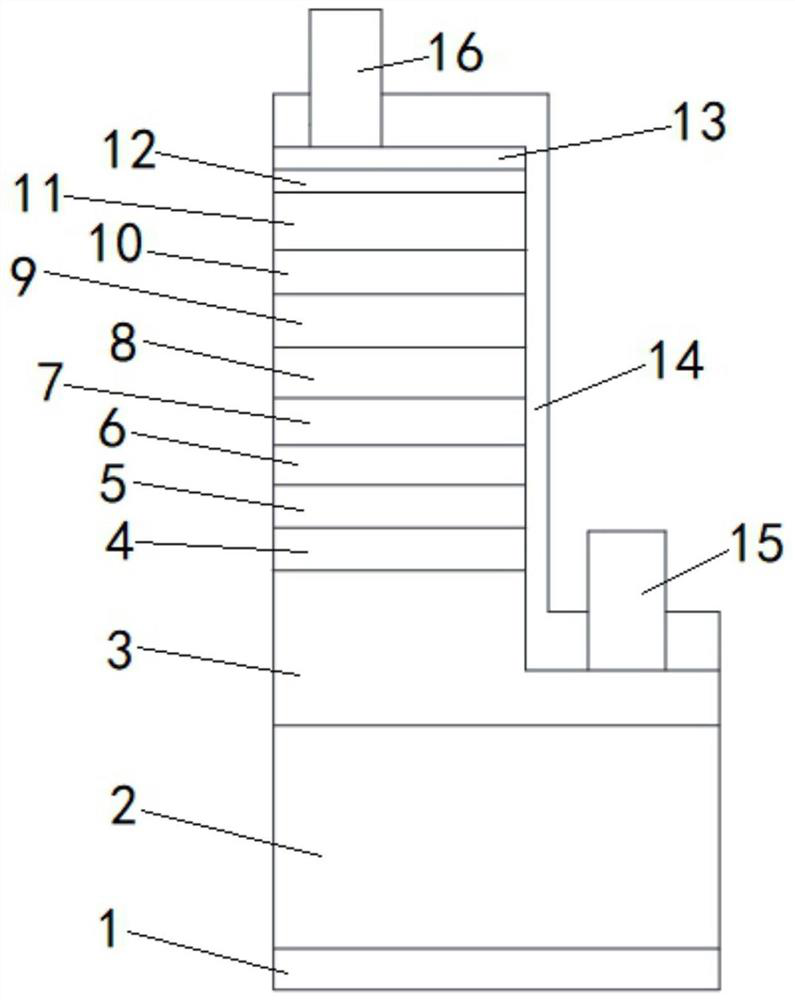
[0030] see figure 1 , a method for growing an LED epitaxial structure. This embodiment is applied to improving the luminous brightness of the LED epitaxial structure.

[0031] A method for growing an LED epitaxial structure, comprising sequentially growing a first GaN layer 2, a second GaN layer 3, a third GaN layer 4, a first superlattice layer 5, a second superlattice layer 6, The light emitting layer, the first P-type GaN layer 9, the P-type AlGaN layer 10, the second P-type GaN layer 11 and the third P-type GaN layer 12, such as figure 1 shown.

[0032]In this application, MOCVD (metal organic compound chemical vapor deposition) is used to grow high-brightness GaN-based LED epitaxial structures, and high-purity H 2 , high purity N 2 At least one of them is used as a carrier gas; high-purity NH is used 3 (Ammonia) as N source; metal-organic source trimethylgallium (TMGa) or triethylgallium (TEGa) as gallium source; trimethylindium (TMIn) as indium source; trimethylalumi...

Embodiment 2

[0056] The difference between this embodiment and Embodiment 1 is that in Step 5, when growing the first superlattice layer 5, N-type GaN doped with Si and In not doped with Si are alternately grown. x Ga (1-x) N, the number of alternate growth cycles is 10, and the obtained whole chip particle is sample 2.

Embodiment 3

[0058] The difference between this embodiment and Embodiment 1 is that in Step 5, when growing the first superlattice layer 5, N-type GaN doped with Si and In not doped with Si are alternately grown. x Ga (1-x) N, the number of alternate growth cycles is 8, and the obtained whole chip particles are sample 3.


PUM


Abstract

The invention provides an LED epitaxial structure growth method, which comprises the following steps: sequentially growing a first GaN layer, a second GaN layer, a third GaN layer, a first superlattice layer, a second superlattice layer and a light-emitting layer on a substrate, wherein the growth process of the first superlattice layer is that Si-doped N-type GaN and Si-undoped InxGa1-xN alternately grow, x is equal to 0.10-0.15, and the number of alternate growth cycles is 6-10. The invention further provides an LED epitaxial structure, which comprises a substrate, a first GaN layer, a second GaN layer, a third GaN layer, a first superlattice layer, a second superlattice layer, a light-emitting layer, a first P-type GaN layer, a P-type AlGaN layer, a second P-type GaN layer and a third P-type GaN layer which are stacked from bottom to top. According to the invention, the distribution of Si in a third GaN layer, a first superlattice layer and a second superlattice layer is utilized, so that the capacitance of the epitaxial structure is enlarged, and the number of effective electrons in the LED epitaxial structure is increased.

Description

technical field [0001] The invention relates to the technical field of LED manufacturing, in particular to an LED epitaxial structure and a growth method thereof. Background technique [0002] LED is a solid-state lighting device. It is recognized by consumers because of its small size, low power consumption, long service life, high brightness, environmental protection, and durability. Therefore, the scale of domestic LED production is also gradually expanding; the market The quality of LED products in demand is getting higher and higher. What customers are concerned about is that LEDs are more energy-efficient, have higher brightness and better light efficiency, which puts forward higher requirements for the growth of LED epitaxial structures; high-power device driving voltage and brightness Requirements are the focus of current market demand. [0003] To sum up, there is an urgent need for an LED epitaxial structure and a growth method thereof to solve the problems existi...

Claims


Application Information

Patent Timeline
IPC IPC(8): H01L33/00H01L33/06H01L33/32C30B25/02C30B25/16C30B29/40C30B29/68
CPCH01L33/007H01L33/06H01L33/325C30B29/68C30B29/406C30B29/403C30B25/02C30B25/16
Inventor 冯磊徐平
Owner XIANGNENG HUALEI OPTOELECTRONICS
Learn More