Manufacturing method of multilayer board blind hole buried hole filling packaging substrate

A technology for packaging substrates and manufacturing methods, which is applied in the manufacture of printed circuits, coating of non-metallic protective layers, and processing of insulating substrates/layers, etc. Substrate functionality, reliability and other issues, to achieve good blind hole filling effect, improve functionality and reliability effects

Active Publication Date: 2021-07-23
江门市和美精艺电子有限公司
View PDF4 Cites 2 Cited by
  • Summary
  • Abstract
  • Description
  • Claims
  • Application Information

AI Technical Summary

Problems solved by technology

In the existing manufacturing process, the blind / buried multi-layer board is connected with the plating hole in the outer layer circuit and the adjacent inner layer, and the plating hole is filled with conductive materials, and the bonding force between the bottom of the blind hole and the substrate is insufficient, resulting in microcracks in some places In this way, the yield rate of the packaged substrates filled with holes after packaging is very low during the test, and the resistance value of the through holes corresponding to the place where there is resistance changes very greatly. Normal power-on, normal resistance, long-term power-on, about After 10 hours, the resistance value will become infinite, and some products will return to normal function after power failure, but some products will not recover, which will affect the functionality and reliability of the packaging substrate.
Moreover, the hole filling effect of different blind hole diameters is different

Method used


Image

  • Manufacturing method of multilayer board blind hole buried hole filling packaging substrate
  • Manufacturing method of multilayer board blind hole buried hole filling packaging substrate
  • Manufacturing method of multilayer board blind hole buried hole filling packaging substrate

Examples


Embodiment Construction

[0061] The preferred embodiments of the present invention will be further described in detail below.

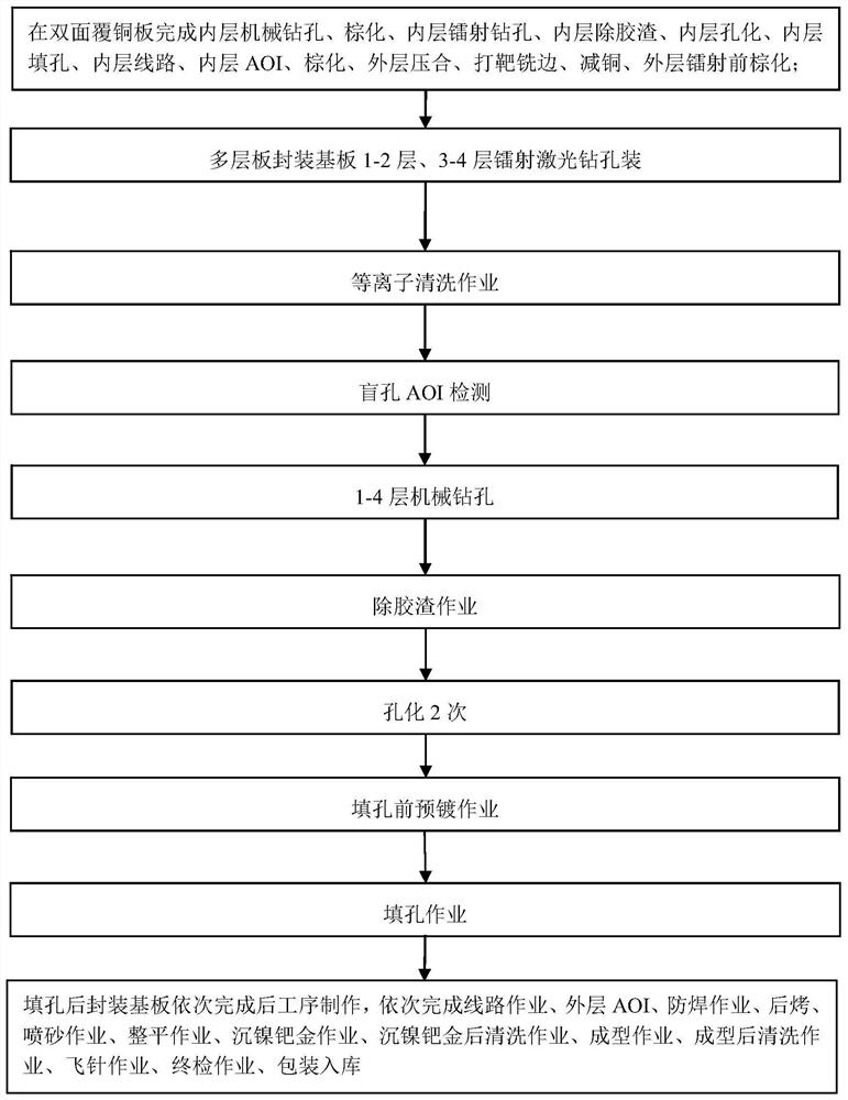
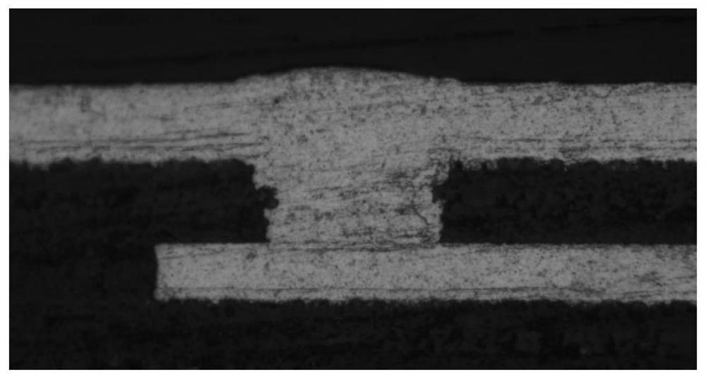
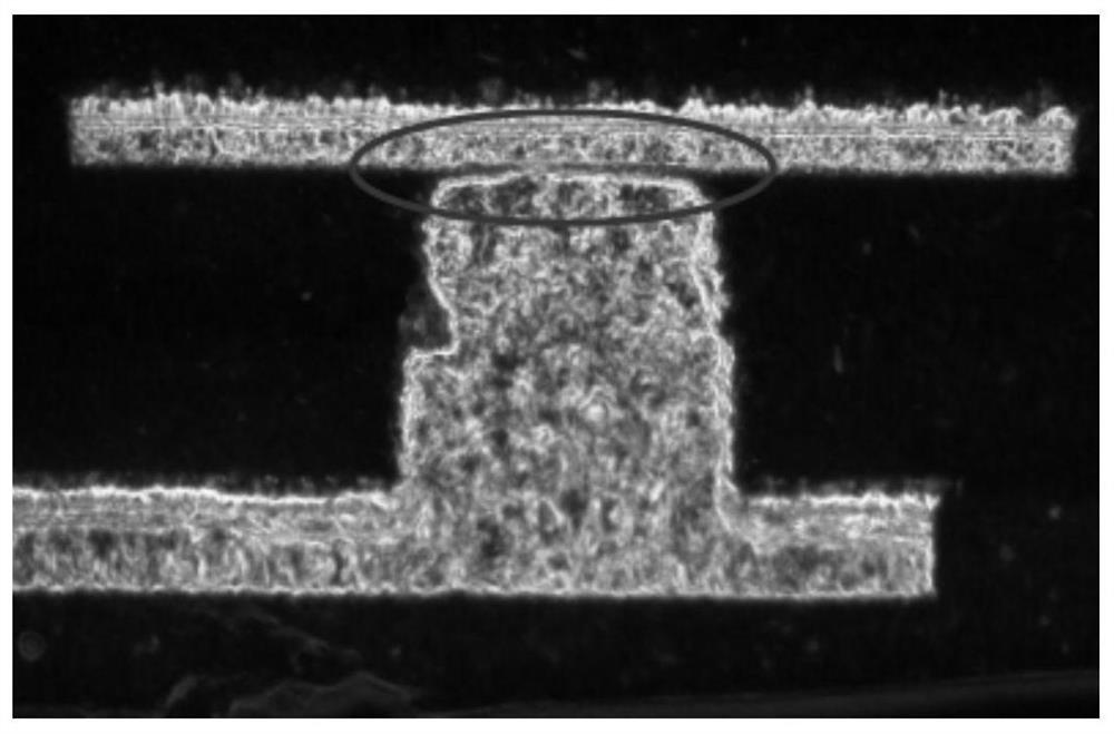
[0062] A method for manufacturing a multilayer board blind hole buried hole filling process packaging substrate, such as figure 1 shown, including the following steps:

[0063] 1. Prepare double-sided copper clad laminates, complete inner layer mechanical drilling, browning, inner layer laser drilling, inner layer desmearing, inner layer holeization, inner layer hole filling, inner layer wiring, inner layer AOI, browning Melting, outer layer lamination, target milling, copper reduction, outer layer pre-laser browning, outer layer laser drilling.

[0064] This step is the process flow of the package substrate before the embodiment, in which the double-sided copper-clad laminate is the inner layer cutting board, and the thickness of the core board is in the range of 0.04mm-0.1mm (such as 0.04mm, 0.06mm, 0.08mm, 0.1mm, etc. thickness), Among them, the thickness of the bottom c...


PUM

PropertyMeasurementUnit
thicknessaaaaaaaaaa

Abstract

The invention provides a manufacturing method of a multilayer board blind hole, buried hole and filled hole packaging substrate. The method comprises the following steps: performing inner layer mechanical drilling, browning, inner layer laser drilling, inner layer glue residue removal, inner layer holing, inner layer hole filling, inner layer circuit, inner layer AOI, browning, outer layer pressing, targeting and edge milling, copper reduction, outer layer laser pre-browning and outer layer laser drilling on a double-sided copper-clad plate to obtain a packaging substrate; performing plasma cleaning on the packaging substrate and blind holes; drilling a non-conducting positioning hole in the packaging substrate; carrying out glue residue removal treatment on the packaging substrate to remove glue residues in the holes and on the surface of the packaging substrate; carrying out hole processing on the packaging substrate, forming a layer of conductive film on the hole wall of the blind hole, and enabling the outermost two layers on the two surfaces of the packaging substrate to be connected through the conductive film in the blind hole and to be connected with the buried hole in the inner layer; and carrying out blind hole filling treatment. By adopting the technical scheme of the invention, the functionality and reliability of the packaging substrate are improved, and a better blind hole filling effect is obtained.

Description

technical field [0001] The invention belongs to the technical field of packaging substrate preparation, and in particular relates to a method for manufacturing a multilayer board blind hole-filling packaging substrate. Background technique [0002] With the rapid development of the circuit board industry, the continuous growth of the output of electronic communication equipment, electronic computers, household appliances and other electronic products has provided a strong impetus for the rapid growth of the circuit board industry. There is a large demand for servers, storage, and network equipment, and packaging substrates are the basic electronic components. The packaging substrate line width / spacing, miniaturization of blind hole aperture, and high-level thin media are the future development trends of HDI high integration. In the existing manufacturing process, the blind / buried multi-layer board is connected with the plating hole in the outer layer circuit and the adjacent...

Claims


Application Information

Patent Timeline
Patent Type & Authority Applications(China)
IPC IPC(8): H05K3/42H05K3/00H05K3/28H05K3/26
CPCH05K3/42H05K3/0047H05K3/0055H05K3/28H05K3/26
Inventor 张必燕
Owner 江门市和美精艺电子有限公司
Why Eureka
Try Eureka